Download
1 / 1
10 likes | 150 Views
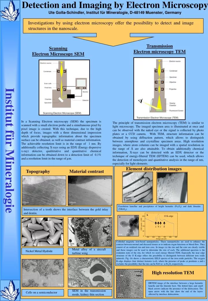
Detection and Imaging by Electron Microscopy. Institut für Mineralogie. 1 µm. 20 nm. 100µm. 100µm. 100nm. b. O K-edge. a. b. c. d. 2µm. ilm. 10µm. 2 nm. Ute Golla-Schindler, Institut für Mineralogie, D-48149 Muenster, Germany.

E N D
Detection and Imaging by Electron Microscopy Institut für Mineralogie 1 µm 20 nm 100µm 100µm 100nm b O K-edge a b c d 2µm ilm 10µm 2 nm Ute Golla-Schindler, Institut für Mineralogie, D-48149 Muenster, Germany Investigations by using electron microscopy offer the possibility to detect and image structures in the nanoscale. Transmission Electron microscopy TEM Scanning Electron Microscopy SEM In a Scanning Electron microscopy (SEM) the specimen is scanned with a small electron probe and a simultaneous pixel by pixel image is created. With this technique, due to the high depth of focus, images with a three dimensional impression which provide topographic information about the specimen surface can be obtained, as well as material contrast information. The achievable resolution limit is in the range of 1 nm. By additionally collecting X-rays using an EDX (Energy dispersive x-ray) detector, qualititative and quantitative chemical information can be obtained down to a detection limit of 0.1% and a resolution limit in the range of µm. The principle of transmission electron microscopy (TEM) is similar to light microscopy. The imaged specimen area is illuminated at once and can be observed with the naked eye or the signal is collected by photo plates or a CCD camera. With TEM, structure information can be obtained by using diffraction pattern, which allows to distinguish between amorphous and crystalline specimen areas. High resolution images, where atom columns can be imaged with a spatial resolution in the range of Å are also attainable. To obtain additionally chemical information, X-rays can be detected with an EDX detector or the technique of energy-filtered TEM (EFTEM) can be used, which allows the detection of monolayers and quantitative analysis in the range of nm, especially for light elements. Element distribution images Topography Material contrast Exsolution lamellae and precipitates of bright hematite (Fe3O4) and dark ilmenite (TiFeO4). Intersection of a tooth shows the interface between the gold inlay and dentin. a Collodial magnetic iron-based nanoparticles. These nanoparticles are used to enhance the contrast between normal and diseased tissues or to indicate organ functions or blood flow. They consist of an oxidized rim and iron core. In image (a) the rim and the core are clearly visible and those images can be used to determine the size of each. The additional question is the oxidation state of the rim, for which we used energy filtered TEM. Especially the near edge structure of the O K-edge offers the possibility to distinguish between different iron oxide minerals. Fig. (b) shows a characteristic EELS spectra of the iron oxide particles. The oxygen K-edge displays four distinct features (a-d), where the presence of peaks at positions a and c excludes the possibility that the rim can be FeO or -Fe2O3 respectively. Metal alloy of a aircraft turbine wing Nickel Metal Hydride High resolution TEM HRTEM image of the interface between a large hematite lamella and the ilmenite host. The dotted lines and small black arrows indicate the presence of the dislocation. The open arrow with the line show the end of the layers affected by interface dislocations. SEM in the transmission mode, kidney thin section Cells on a semiconductor