Download
1 / 2
20 likes | 23 Views
We are at the edge of advances and ensures you can reap the benefits of the most revolutionary<br>developments. Visit our site at https://parksystems.com/ and explore our wide range of technology.

E N D
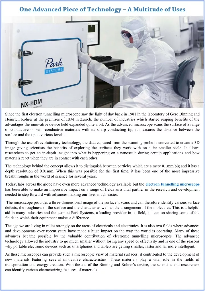
O n e A d v a n c e d P i e c e o f T e c h n o l o g y – A Mu l t i t u d e o f U s e s Since the first electron tunnelling microscope saw the light of day back in 1981 in the laboratory of Gerd Binning and Heinrich Rohrer at the premises of IBM in Zürich, the number of industries which started reaping benefits of the advantages the innovative device held expanded quite a bit. As the advanced microscope scans the surface of a range of conductive or semi-conductive materials with its sharp conducting tip, it measures the distance between the surface and the tip at various levels. Through the use of revolutionary technology, the data captured from the scanning probe is converted to create a 3D image giving scientists the benefits of exploring the surfaces they work with on a far smaller scale. It allows researchers to get an in-depth insight into what is happening on a nanoscale during certain applications and how materials react when they are in contact with each other. The technology behind the concept allows it to distinguish between particles which are a mere 0.1mm big and it has a depth resolution of 0.01mm. When this was possible for the first time, it has been one of the most impressive breakthroughs in the world of science for several years. Today, labs across the globe have even more advanced technology available but the electron tunnelling microscope has been able to make an impressive impact on a range of fields as a vital partner in the research and development needed to step forward with advances making our lives much easier. The microscope provides a three-dimensional image of the surface it scans and can therefore identify various surface defects, the roughness of the surface and the character as well as the arrangement of the molecules. This is a helpful aid in many industries and the team at Park Systems, a leading provider in its field, is keen on sharing some of the fields in which their equipment makes a difference. The age we are living in relies strongly on the areas of electricals and electronics. It is also two fields where advances and developments over recent years have made a huge impact on the way the world is operating. Many of these advances became possible by the valuable contribution of electronic tunnelling microscopes. The advanced technology allowed the industry to go much smaller without losing any speed or effectivity and is one of the reasons why portable electronic devices such as smartphones and tablets are getting smaller, faster and far more intelligent. As these microscopes can provide such a microscopic view of material surfaces, it contributed to the development of new materials featuring several innovative characteristics. These materials play a vital role in the fields of transportation and energy creation. With the aid of the Binning and Rohrer’s device, the scientists and researchers can identify various characterizing features of materials.
These are attributes such as the magnetic, mechanical and electrical properties and how it can be functional in areas of manufacturing such as aviation, the automobile industry and even the generation of electricity. As you can study surfaces and the defects in material, the device also allows researchers and scientist to explore friction in far greater depth. It allows them to see on a nano-level what is happening with the material when it meets each other. These observations play a vital role in the development of conductors and microelectronics. It is often the case that we go about in our everyday lives, enjoying everyday comforts and living life with all its advances and outstanding developments. While we are so blasé regarding all the research and development that goes into our life luxuries, it is a good reminder that there has been some outstanding work done by heroes such as Benning and Rohrer. Work which made it possible for industries to create the comforts we are used to. About Us: Our commitment to you is to find the solutions to challenges holding back the development and research in a range of fields. It is why we spend endless hours to ensure quality and service and above all, make sure we can guarantee precision and accuracy in all our prestige options. As a global role-player in the industry with offices worldwide, you can be sure to rely on our support and outstanding customer service. Park Systems is a leader in the field of microscopic exploration, we are at the edge of advances and ensures you can reap the benefits of the most revolutionary developments. Visit our site at https://parksystems.com/ and explore our wide range of technology.