Download
1 / 2
20 likes | 37 Views
Staying up to date on the most modern microscopy products can be difficult as they are constantly evolving and advancing their capabilities. A new advancement in the researching world is scanning probe microscopes, which essentially include techniques fount in both scanning tunneling microscopes and atomic force microscopes. Most labs and researchers are familiar with these styles of devices but have yet to use SPM which combines the two methods. This opens a new style of research that has been nearly impossible in the past.

E N D
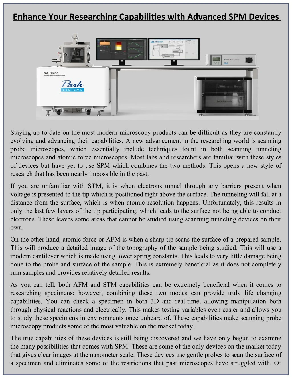
Enhance Your Researching Capabilities with Advanced SPM Devices Staying up to date on the most modern microscopy products can be difficult as they are constantly evolving and advancing their capabilities. A new advancement in the researching world is scanning probe microscopes, which essentially include techniques fount in both scanning tunneling microscopes and atomic force microscopes. Most labs and researchers are familiar with these styles of devices but have yet to use SPM which combines the two methods. This opens a new style of research that has been nearly impossible in the past. If you are unfamiliar with STM, it is when electrons tunnel through any barriers present when voltage is presented to the tip which is positioned right above the surface. The tunneling will fall at a distance from the surface, which is when atomic resolution happens. Unfortunately, this results in only the last few layers of the tip participating, which leads to the surface not being able to conduct electrons. These leaves some areas that cannot be studied using scanning tunneling devices on their own. On the other hand, atomic force or AFM is when a sharp tip scans the surface of a prepared sample. This will produce a detailed image of the topography of the sample being studied. This will use a modern cantilever which is made using lower spring constants. This leads to very little damage being done to the probe and surface of the sample. This is extremely beneficial as it does not completely ruin samples and provides relatively detailed results. As you can tell, both AFM and STM capabilities can be extremely beneficial when it comes to researching specimens; however, combining these two modes can provide truly life changing capabilities. You can check a specimen in both 3D and real-time, allowing manipulation both through physical reactions and electrically. This makes testing variables even easier and allows you to study these specimens in environments once unheard of. These capabilities make scanning probe microscopy products some of the most valuable on the market today. The true capabilities of these devices is still being discovered and we have only begun to examine the many possibilities that comes with SPM. These are some of the only devices on the market today that gives clear images at the nanometer scale. These devices use gentle probes to scan the surface of a specimen and eliminates some of the restrictions that past microscopes have struggled with. Of
course, as with all types of technology, there are some basic disadvantages that come with the many advantages. A huge benefit of scanning probe microscopes is the lack of preparation time that comes with getting your specimen ready. These devices can research a variety of specimens and observe them in a large range of environments. You can purchase modified and improved SPM devices that can give you efficient and fast images with little efforts. On the other hand, there are some disadvantages to these devices, with the biggest being the resolution of the images produced. Images are in gray or black and white only. This can lead to some unclear characteristics that are not portrayed as accurately as possible. There are ways to use computer programs to make these images colored, but this adds more time to your researching and can still produce some inaccuracies. Overall, the use of scanning probe microscopy in a modern laboratory has opened up capabilities that have previously been unheard of. It combines some of the most advanced forms of research on the market today to give quality, diverse images of a variety of samples in various environments. This is an excellent choice when considering what to add to your lab as it widens your researching capabilities and keeps you competitive with other labs today. About Us: Park Systems is a leading manufacturer of atomic force microscopy systems with a full range of products. Multiple industries, such as engineers in chemistry, materials, physics, life sciences, semiconductor, and data storage can benefit from their range of supplies. The products produced by Park Systems are represented in thousands of institutions and businesses worldwide. The main headquarters for this company is based in Santa Clara, California, but products produced are sold and supported worldwide with the many regional offices throughout the world. Each of Park Systems products are sold at the lowest operating cost, with high data accuracy, and superior productivity. To learn more about their products, please visit their website:http://www.parkafm.com 3040 Olcott Street Santa Clara, CA United States (95054) Contact Us: 408-986-1110 (http://www.parksystems.com)