Download
1 / 43
470 likes | 714 Views
4. Operational Amplifiers. CIRCUITS by Ulaby & Maharbiz. Overview. Tech Brief 7: IC Fabrication. Wafer : Thin slice of semiconductor material with highly polished surface Processed wafer is cut into many dies or chips. Lithography : Defining spatial pattern

E N D
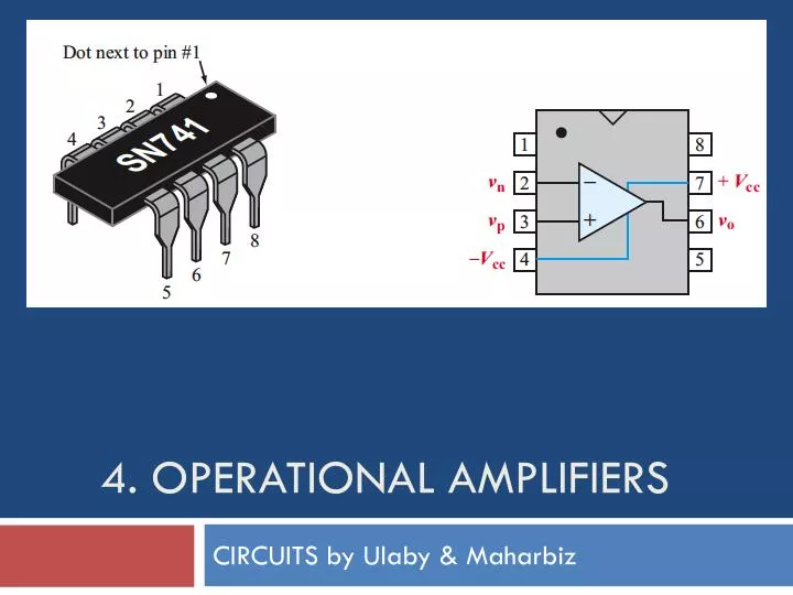
4. Operational Amplifiers CIRCUITS by Ulaby & Maharbiz
Tech Brief 7: IC Fabrication Wafer: Thin slice of semiconductor material with highly polished surface Processed wafer is cut into many dies or chips. Lithography: Defining spatial pattern Photoresist: Polymer material that does not allow etching or deposition of areas underneath it.
Tech Brief 7: IC Fabrication Lithography: Defining spatial pattern Photoresist: Polymer material that does not allow etching or deposition of areas underneath it.
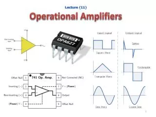
Operational Amplifier “Op Amp” • Two input terminals, positive (non- inverting) and negative (inverting) • One output • Power supply V+ , and Op Amp with power supply not shown (which is how we usually display op amp circuits) Op Amp showing power supply
Gain • Key important aspect of op amp: high voltage gain • Output , A is op-amp gain (or open-loop gain) – different from circuit gain G • Linear response
Example 4-1: Op Amp Amplifier KCL at Node a: Node a KCL at Node b: Node b For infinite A: = 5 = 4.999975
Negative Feedback • Feedback: return some of the output to the input • Negative feedback decreases input signal • Achieves desired circuit gain, with wide range for input Negative Feedback No Feedback Range of Range of 5 Gain = 5 Range of : ‒2 V to +2 V : ‒10 mV to +10 mV Range of Gain = 1million
Circuit Analysis With Ideal Op Amps • Use nodal analysis as before, but with “golden rules” • N • Do not apply KCL at op amp output No voltage drop across op amp input No current into op amp
Noninverting Amplifier At node (max) = Vcc
Example 4-2: Input Current Source Relate output voltage to input current source
Example 4-4: Solution:
Difference Amplifier Note negative gain of channel 1
Voltage Follower “Buffers” Sections of Circuit depends on both input and load resistors is immune to input and load resistors What is the op amp doing?
Example 4-5: Elevation Sensor h = elevation, inversely proportional to air pressure Sensor Response Desired Output
Measurement Uncertainty Direct Measurement v2 V0 = V2 ± 1% of V2 Thermistor (T = 21°C) G = 1 ± 1% 21°C ± 0.21°C Differential Measurement v2 G = 1 1% V0 = (V2‒ V1) ±1% of (V2‒ V1) Thermistor (T = 21°C) 1°C ±0.01°C v1 Much better measurement uncertainty Fixed Reference Temp = 20°C
Instrumentation Amplifier Highly sensitive differential amplifier
Digital to Analog Converter Converts digital value into analog voltage 4-digit example
Digital to Analog Converter Represent digital value with analog voltage
MOSFET (Field Effect Transistor) Active Device: Voltage Controlled Current Source Gate voltage controls drain/source current
MOSFET Equivalent Circuit Characteristic curves Idealized response
Example 4-9: MOSFET Amplifier Given: Determine
Load Line You can use a “load line” to graphically determine Vout = VDSfor a given Vin = VGS VDD/RD RL VDD
VDD= 15 V 15 RL 10 out =V D ID DS G V In Out S 5 0 1 1 0 In Out 0 0 1 2 3 4 5 V =V GS in Digital Circuit: MOSFET Inverter VDD Output “High” Logic 1 Output “High” Logic 1 Output “Low” Logic 0 Output “Low” Logic 0 Input “Low” Input “High”
Read-Only Memory (ROM) Circuits VREAD = 1 VBIT = 0100
A B Out 0 0 1 0 1 1 1 0 1 1 1 0 A Out B Another Digital Circuit Element: NAND No current flows through resistor, unless both A and B inputs turn their transistors on to “pull down” Vout VDD Vout A B NAND gates can be used to build any binary logic function
A B Out 0 0 1 0 1 0 1 0 0 1 1 0 A Out B Another Digital Circuit Element: NOR Current will flow if either A or B inputs turn their transistors on to “pull down” Vout VDD Vout A B NOR gates can be used to build any binary logic function