Download
1 / 1
20 likes | 145 Views
High- Dielectric for Flexible Displays using Anodized Tantalum Pentoxide Jovan Trujillo Advisor: Dr. Gregory B. Raupp Department of Chemical Engineering Arizona State University Flexible Display Center 4-20-07. 60 mA process. 20 mA process. 60 mA ramp to 100 V. The FDC group:

E N D
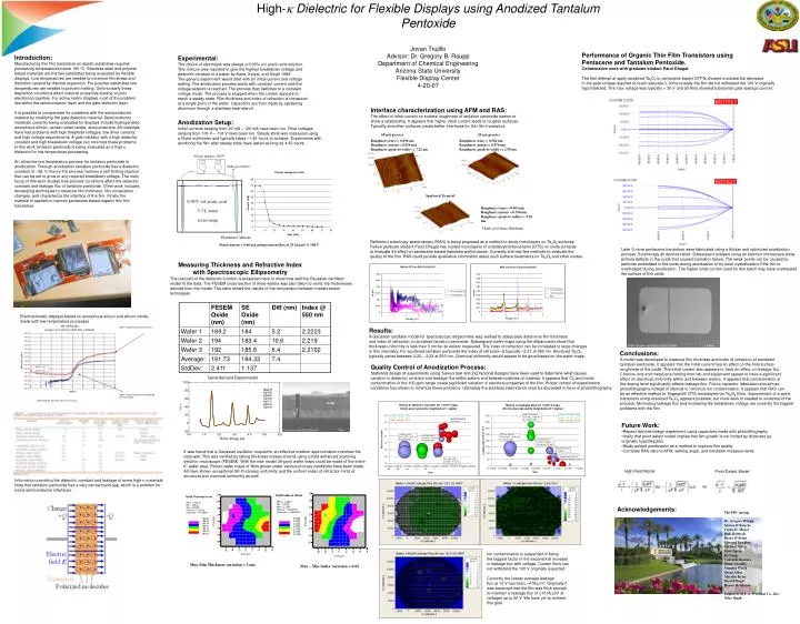
High- Dielectric for Flexible Displays using Anodized Tantalum Pentoxide Jovan Trujillo Advisor: Dr. Gregory B. Raupp Department of Chemical Engineering Arizona State University Flexible Display Center 4-20-07 60 mA process 20 mA process 60 mA ramp to 100 V The FDC group: Dr. Gregory Raupp Shawn O’Rourke Curtis D. Moyer Dirk Bottesch Barry O’Brien Edward Bawolek Michael Marrs Scott Ageno Ke Long Consuelo Romero Diane Carrillo Virginia Woolf Susan Allen Marilyn Kyler Parul Dhagat Hanna Heikkinen Engineers at J. A. Woollam Co., Inc.: Neha Singh Roughness (rms) = 0.696 nm Roughness (mean) = 0.516 nm Roughness (peak-to-valley) = 7.22 nm Roughness (rms) = 0.564 nm Roughness (mean) = 0.476 nm Roughness (peak-to-valley) = 2.99 nm Hydrogen bubbles 0.05% vol acetic acid 5.5 L water Sputtered Ta metal room temp. Roughness (rms) = 0.463 nm Roughness (mean) = 0.334 nm Roughness (peak-to-valley) = 3.36 nm Platinum Cathode Final current < 0.40 mA giving current flux of 25 fA/m2 @ 100 V Thank you Hanna Heikkinen Electrophoretic displays based on amorphous silicon and silicon nitride, made with low temperature processes. High- should increase drive current. High- should reduce threshold voltage (increase slope). Typical log(Ids)-Vgs data from our transistors. Performance of Organic Thin Film Transistors using Pentacene and Tantalum Pentoxide. Collaborative work with graduate student Parul Dhagat. The first attempt at apply anodized Ta2O5 to pentacene based OTFTs showed a substantial decrease in the gate voltage required to reach saturation. Unfortunately the film did not withstand the 100 V originally hypothesized. The max voltage was typically < 30 V and all films showed substantial gate leakage current. Introduction: Manufacturing thin film transistors on elastic substrates requires processing temperatures below 180 oC. Stainless steel and polymer based materials are the two substrates being evaluated for flexible displays. Low temperatures are needed to minimize film stress and distortion caused by thermal expansion. For polymer substrates low temperatures are needed to prevent melting. Unfortunately these deposition conditions affect material properties leading to poor electrical properties. For active matrix displays most of the problem lies within the semiconductor layer and the gate dielectric layer. It is possible to compensate for problems with the semiconductor material by modifying the gate dielectric material. Semiconductor materials currently being evaluated for displays include hydrogenated amorphous silicon, certain metal oxides, and pentacene. All materials have had problems with high threshold voltages, low drive currents, and high voltage requirements. A gate insulator with a high dielectric constant and high breakdown voltage can minimize these problems. In this work tantalum pentoxide is being evaluated as a high- dielectric for low temperature processing. An attractive low temperature process for tantalum pentoxide is anodization. Through anodization tantalum pentoxide has a dielectric constant of ~28. In theory the process involves a self limiting reaction that can be set to grow to any required breakdown voltage. The main focus of this work studies how process conditions affect the dielectric constant and leakage flux of tantalum pentoxide. Other work includes developing techniques to measure film thickness, film composition changes, and characterize the interface of the film. Finally the material is applied to improve pentacene based organic thin film transistors. Experimental: The choice of electrolyte was always a 0.05% v/v acetic acid solution. This mixture was reported to give the highest breakdown voltage and dielectric constant in a paper by Kalra, Katyal, and Singh 1989. The generic experiment would start with an initial current and voltage setting. The anodization process starts with constant current until the voltage setpoint is reached. The process then switches to a constant voltage mode. The process is stopped when the current appears to reach a steady state. Film thickness and index of refraction is measured at a single point of the wafer. Capacitors are then made by sputtering aluminum through a stainless steel stencil. Interface characterization using AFM and RAS: The effect of initial current on surface roughness of tantalum pentoxide seems to show a relationship. It appears that higher initial current leads to rougher surfaces. Typically smoother surfaces create better interfaces for thin film transistors. Anodization Setup: Initial currents ranging from 20 mA – 120 mA have been run. Final voltages ranging from 100 V – 118 V have been run. Steady state was measured using a Fluke multimeter and typically takes ~1:40 hours to achieve. Experiments with anodizing the film after steady state have lasted as long as 4:30 hours. Reflection anisotropy spectroscopy (RAS) is being proposed as a method to study monolayers on Ta2O5 surfaces. Fellow graduate student Parul Dhagat has coated monolayers of octaldecytrichlorosilanol (OTS) on oxide surfaces to evaluate it’s effect on pentacene based transistor performance. Currently she has few methods to evaluate the quality of the film. RAS could provide qualitative information about such surface treatments on Ta2O5 and other oxides. Later 5 more pentacene transistors were fabricated using a thicker and optimized anodization process. Surprisingly all devices failed. Subsequent analysis using an electron microscope show pinhole defects in the oxide that caused transistor failure. The weak points can be caused by particles embedded in the oxide during anodization or by local crystallization if the film is overheated during anodization. The higher initial current used for this batch may have overheated the surface of the oxide. Measuring Thickness and Refractive Index with Spectroscopic Ellipsometry The real part of the dielectric function is presented here to show how well the Gaussian oscillator model fit the data. The FESEM cross-section of three wafers was also taken to verify the thicknesses derived from the model. The table shows the results of the comparison between measurement techniques. Results: A Gaussian oscillator model for spectroscopic ellipsometry was verified to adequately determine film thickness and index of refraction on anodized tantalum pentoxide. Subsequent wafer maps using the ellipsometer show that thickness uniformity is less than 3 nm for all wafers measured. The index of refraction can be correlated to large changes in film chemistry. For sputtered tantalum pentoxide the index of refraction is typically ~2.21 at 550 nm. Anodized Ta2O5 typically varies between 2.22 – 2.23 at 550 nm. Chemical uniformity would appear to be good based on the wafer maps. Conclusions: A model was developed to measure film thickness and index of refraction of anodized tantalum pentoxide. It appears that the initial current has an effect on the final surface roughness of the oxide. The initial current also appears to have an effect on leakage flux. Chlorine ions and metal ions coming from lab and equipment appear to have a significant effect on electrical uniformity within and between wafers. It appears that contamination at the doping level significantly affects leakage flux. Future capacitor fabrication should use photolithography instead of stencils to minimize ion contamination. It appears that RAS can be an effective method to ‘fingerprint’ OTS monolayers on Ta2O5 films. Improvement of organic transistors using anodized Ta2O5 appears possible, but more work is needed to understand the process. Minimizing leakage flux and increasing the breakdown voltage are currently the biggest problems with the film. Quality Control of Anodization Process: Statistical design of experiments using Tukey’s test and 2x2 factorial designs have been used to determine what causes variation in dielectric constant and leakage flux within wafers and between batches of material. It appears that Cl2 and metal contamination in the 100 ppm range cause significant variation in electrical properties of the film. Proper control of experimental conditions has shown to minimize these problems. Ultimately the stainless steel stencil must be discarded in favor of photolithography. • Future Work: • Repeat factorial design experiment using capacitors made with photolithography. • Verify that point defect model implies that film growth is not limited by thickness as • originally hypothesized. • Study pulsed anodization as a method to improve film quality. • Correlate RAS data to AFM, wetting angle, and transistor measurements. It was found that a Gaussian oscillator coupled to an effective medium approximation matched the data well. This was verified by taking thickness measurements using a field enhanced scanning electron microscope (FESEM). With the new model 39-point wafer maps could be made of the entire 6” wafer area. Eleven wafer maps of films grown under various process conditions have been made. All have shown exceptional film thickness uniformity and the uniform index of refraction hints at structural and chemical uniformity as well. High Field Model Point Defect Model Information providing the dielectric constant and leakage of some high- materials. Note that tantalum pentoxide has a very narrow band gap, which is a problem for some semiconductor interfaces. vs Acknowledgements: Ion contamination is suspected of being the biggest factor in the exponential increase in leakage flux with voltage. Current films can not withstand the 100 V originally expected. Currently the lowest average leakage flux at 10 V has been ~4 fA/m2. Originally it was expected that the film was thick enough to maintain a leakage flux of <10 fA/m2 at voltages up to 50 V. We have yet to achieve this goal. Max-Min Thickness variation < 3 nm Max – Min Index variation < 0.02