Download
1 / 35
360 likes | 514 Views
Design of EMI-Suppressing Power Supply Regulator for Automotive electronics. October 11th, 2006. Junfeng Zhou Promotor: Prof. Wim Dehaene KULeuven ESAT-MICAS. Outline. Part I : Introduction Part II : Low Noise Power Supply–EMI-Suppressing Regulator Principles Design Simulation

E N D
Design of EMI-Suppressing Power Supply Regulator for Automotive electronics October 11th, 2006 Junfeng Zhou Promotor: Prof. Wim Dehaene KULeuven ESAT-MICAS
Outline • Part I: Introduction • Part II: Low Noise Power Supply–EMI-Suppressing Regulator • Principles • Design • Simulation • Calculation • Chip Details • Measured Results • Part III: Possible Improvements • Part IV: Future work
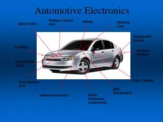
Part I: Introduction • Electro-Magnetic Interference (EMI) and radiated emission have become a major problem for automotive electronics, • Radiated emission is mostly a consequence of di/dt on the supply lines. • Although the detailed calculation of EMI noise is rather difficult , we can use the di/dtas the index, since the current loop contributes the EMI.
Part II: EMI-Suppressing Regulator Previous research on Low Noise Logic Families shows that 2 major problems still remain: • Static power consumption • New logic family standard cell library must be designed and characterised. (large NRE cost, risk) ? Any global approach ?
Principles • 1. Current source ensures the major di/dt reduction • 2. Slow varying • is key to EMC success • 3. Minimize the static current Diagram of EMI-Suppressing Regulator
EMI-Suppressing Regulator – basic structure Determine the switching speed, Hence determine the di/dt Energy reservoir
Why new structure ? Simple Driving capability Miller effect on compensation capacitor Cascode device
Functionality Simulation & Comparison with standard CMOS di/dt comparison PSD comparison IVbat 44dB w/o EMI-SR and SR IVbat: di/dt p-p = 1.0x10⁷ A/s w/o EMI-SR and SR, di/dt p-p =1.51x10¹¹ A/s di/dt and FFT comparison with standard CMOS
Maple calculation An input current step of 1 mA and 100-ps rise time was used for the calculation and simulation stimulus di/dt I
Stability analysis >3 for > 72° phase margin Approximation: p1 p4 z1 p3 p2 iin Stability ~ Caux/Ctank
Stability analysis – Simulation vs. Calculation Iload =192.7u A φ>72° φ>72° φ≥60° Worst case Stability vs. Iload Stability vs. Iload (26.7u A ~ 72m A) Maple calculation Spectre simulation Raux=1.852K , Caux=20p,Ctank=100p
Current TF analysis H(s)=IVDD(s)/Iin(s) (i.e. di/dt attenuation) dominant pole second pole third pole High frequency zero left half-plane zero
Current TF- simulation vs. calculation Iload =80u A, Raux=1.852K , Ctank=100p dB Maple calculation Spectre simulation - 43 dB - 44 dB
Maximum Attenuation TF vs. Caux dB Cut-off freq. ~ 1/Caux Large attenuation requires Large Ctank and/or small Cdb1 Cascode structure ! Maple calculation - 40 dB Iload =800u A, Raux=1.852K , Ctank=100p
Caux/Ctank and ∆VDDinput ∆VDDinput ~ Caux/Ctank Caux = 4, 8, ..20 pF ∆VDDinput
Design Strategy • EMI-Suppressing Regulator design principles • Stability ~ Caux/Ctank • Time domain ∆VDDinput ~ Caux/Ctank • More stable also means a larger ∆VDDinput • Current TF • Cut-off freq: Gm/Caux • Max. attenuation: Cdb/(Cdb+Ctank) • Design for small Cdb • Similar story possible for Gm, gm • Caution should be exercised to maintain the stability of the EMI-suppressing regulator while designing for higher di/dt reduction
EMC test chip with EMI-Suppressing Regulator Power down block Emergency block SR1 RST Din CLK OUT SR2 RST Din CLK OUT SR9 RST Din CLK OUT SR10 RST Din CLK OUT On-chip LDO SR1, MS-FF, No capa SR6, D-FF, No capa SR2, MS-FF, 1/2 PNMOS capa SR7, D-FF, 1/2 PNMOS capa PD SR3, MS-FF, PNMOS capa SR8, D-FF, PNMOS capa LDO V3v3 PD SR4, MS-FF, PNMOS capa, PWR SR9, D-FF, PNMOS capa, PWR On-chip Serial regulator SR5, MS-FF, PNMOS capa, MIMC capa SR10, D-FF, PNMOS capa, MIMC capa GND VDD_input EMI regulator Ctank Vbat PD
Current source simulation results IVbat V3v3 VDD_input Vctrl Power down enable
Frequency simulation results ~60 dB reduction 40dB (EMI regulator) + 20dB (Serial regulator) 9x10⁶ load current of digital core 7x10³ current of Vbat di/dt of Vbat di/dt of V3v3 FFT FFT di/dt p-p =8.5x10⁴ [A/s] di/dt p-p =1.8x10⁹ [A/s]
Chip Details EMI Suppressing regulator Technology: AMIS 0.35μm I3T80 Area: 1mm x 1.1mm Ctank =100p F Caux = 20 p F Power transistors: Wp=5000 μm Lp= 1 μm (fixed) Supply voltage: 12 V Output voltage: typ. 8V, min.5.5V Quiescent current: 30 μA
Measured Results (2) 8 V Vout 5.78 V 10 ns Iload (0 mA ~ 20 mA ) Load transient response
Measured Results (3) Peak : ~ 5x Trise : ~ 7x di/dtpeak : ~ 24x
Measured Results (4) Peak : ~ 9x Trise : ~ 12x di/dtpeak : ~ 18x
Measured Results (5) di/dt TF di/dt TF -3dB: 1.6 MHz -3dB: 1.8 MHz -33 dB -35 dB IAC injected IAC injected
Conclusions A Low Noise Power Supply Techniques is presented: • Control the way the current delivered to the internal digital core, hence keep the EMI under control, • Comparable reduction on di/dt noise with low noise digital cells only, • More power efficient than the low noise digital cells, • Have similar power consumption to the conventional CMOS logic, • A global approach-Can be adjusted to a wide range of chip size and power consumption level, • Measurement results match the simulation well.
Part III: Possible Improvements peaking H(s)-dB Frequency
Current TF: small signal model z1–Gm/Caux z2– parasitic zero, high frequency p1– Pole at Vctrl: Gm/Caux p2– Pole at VVDD_input: gm/Ctank p3– pole caused by compensation path, high frequency
Current TF: pole-zero tracking z1 cancel off the p1 Make the p2 cut-off frequency This zero is intrinsic for this feedback topology sacrifices dynamic noise performance Make p2 dominant Advanced compensation techniques needed H(s)-dB peaking Options z1 p1 p2 Frequency
Possible solution Key Idea : Achieving Stability Without Sacrificing Dynamic Supply Current Rejection R-C compensation Reduced Gm of OTA Req added for moving the output pole high frequency, also for improvement of the dynamic di/dt rejection
Current TF analysis Req makes p1 and z1 well separated • p1– • p2– • z1– • z2–high frequency
Current TF--Simulation results Peak Freq-3dB Ctank: 100p Iload: 20uA~2m A Gm : 4uA/V RC: 1K Caux: 20p F Raux: 100 K -3dB 632.5 uA 200 uA 63.25 uA 2 mA 20 uA TF vs. ILoad
Part IV: Future Work • Extend the TF measurements into higher frequency, • Find a way to linearly inject the AC current, • Characterization & quantification of EME from digital circuits, • Prediction of EME of digital circuits, • Spread spectrum clock generation.
Questions Thank you for your attention