Download
1 / 62
620 likes | 931 Views
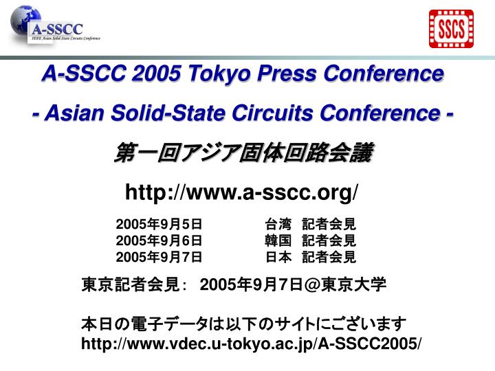
A-SSCC 2005 Tokyo Press Conference - Asian Solid - State Circuits Conference - 第一回アジア固体回路会議 http://www.a-sscc.org/. 2005 年 9 月 5 日 台湾 記者会見 2005 年 9 月 6 日 韓国 記者会見 2005 年 9 月 7 日 日本 記者会見. 東京記者会見: 2005 年 9 月 7 日 @ 東京大学 本日の電子データは以下のサイトにございます http://www.vdec.u-tokyo.ac.jp/A-SSCC2005/.

E N D
A-SSCC 2005 Tokyo Press Conference - Asian Solid-State Circuits Conference - 第一回アジア固体回路会議 http://www.a-sscc.org/ 2005年9月5日 台湾 記者会見 2005年9月6日 韓国 記者会見 2005年9月7日 日本 記者会見 東京記者会見: 2005年9月7日@東京大学 本日の電子データは以下のサイトにございます http://www.vdec.u-tokyo.ac.jp/A-SSCC2005/
開会のご挨拶 A-SSCC概要のご説明 招待講演・パネルのご説明 インダストリープログラムのご説明 各技術分野のご説明 ・アナログ ・Wireless/Wireline ・ディジタル ・メモリ ・システムレベルインテグレーション ・新技術・応用 質疑応答 A-SSCC2005プログラム委員長 桜井 貴康(東京大学) A-SSCC2005プログラム委員長 桜井 貴康(東京大学) Invited Program Chair 黒田 忠広(慶応大学) 黒田 忠広(慶応大学) 各担当 永田 真(神戸大学) 濱田 基嗣(東芝) 荒川 文男(日立) 日高 秀人(ルネサステクノロジ) 池田 誠(東京大学) 野村 昌弘(NEC)、小谷 光司(東北大学) 記者会見次第 15時30分終了予定
A-SSCCとは • IEEE Solid-State Circuits Society (SSCS)主催の4番目*の学会として、Asian Solid-State Circuits Conference (A-SSCC)が今年誕生。アジアに集積回路設計の新しい風を。今後、毎年11月頃アジア地区で開催。 *)昨年までは2月のISSCC (International Solid-State Circuit Conference)、6月のVLSI回路シンポジウム、9月のCICC (Custom Integrated Circuits Conference) の3つ • なぜ、今アジアか • 今後急速に発展するアジア • アジアの学生、研究者、技術者の啓蒙と技術交流の場 • アジアの技術論文の掘り起こし(現存の学会とは競合しない)
IEEERegion 10 IEEEのRegion 10をカバーするA-SSCC A-SSCCの予定 2005年 台湾 大会委員長: Genda Hu (TSMC) 2006年 中国 大会委員長: Ke Gong (清華大学) 2007年 韓国 大会委員長: Chong-Min Kyung (KAIST) 2008年 日本 http://www.ieee.org/organizations/rab/imagemaps/world_reg.html
A-SSCC会議委員会構成 IEEE SSCS AdCom Meetings Committee Steering Committee Ck Wang, G.Hu,W. Sansen, A. Chandrakasan, T.Sakurai, etc Technical Program Committee Takayasu Sakurai, (Japan) Liaison W. Sansen, (Belgium) A. Chandrakasan, (USA) Conference Chair Genda Hu, (Taiwan) Organizing Committee Chien-Wei Jen, (Taiwan) International Professional Management Team ICS Convention Design, Inc. Local: One-year term
プログラム委員会 Chair Takayasu Sakurai , University of Tokyo , Japan Co - Chair Vice - Chair Sung Bae Park , Makoto Ikeda , Samsung University of Electronics , Korea Tokyo , Japan Paper Sections Special Programs Wireless and Wireline Analog Educational Industry Program Communications Beomsup Kim , KAIST , Program Deog - Kyoon Jeong , Nicky Lu , ETRON , H . J . Yoo , KAIST , Korea & Berkana wireless , Seoul National Taiwan USA Korea University , Korea This program is unique to cover “Industry Trend”. Application, demo, evaluation results are more important than originality. Digital Invited Program Memory Liang - Gee Chen , Tadahiro Kuroda , ChangHyun Kim , National Taiwan Keio University , Samsung , Korea University , Taiwan Japan Emerging Applications System - Level Integration and Technologies Hidetoshi Onodera , Siva Narendra , Intel , Kyoto University , Japan USA
A-SSCC2005 • 初回である今年は、”Digital Consumer Age in Asia”というテーマのもと、11月1~3日、台湾 新竹市 アンバサダーホテルにて開催 • アジアへの情報発信、アジアからの情報収集の場 • 産業界のトレンドがわかるインダストリー・プログラム • 世界の講師を招いたチュートリアル • アジアならではの3つの基調講演 • 高倍率の選別を受けたテクニカル論文 • ISSCC、IEEE Journal of Solid-State Circuitとも連携企画
学会会場 台湾 新竹市 Ambassadorホテル 10F, Ambassador Hotel HsinchuAdd : No.188, Chung Hwa Road, Sec 2, Hsinchu 300, Taiwan, R.O.C.TEL : 886-3-515-1111 http://www.ambh.com.tw/
11/3 チュートリアル • 4項目のチュートリアル講演を実施 • Analog/Wireless分野”Analog Circuit Design Towards Nanometer Technologies”M. Steyaert, K.U. Leuven • Digital/Wireline分野”PLL/DLL”C.K. Ken Yang, UCLA • Memory分野”High Performance DRAM Design”Young-Hyun Jun, Samsung • New Technology分野”Crypto Chip Design”Cetin Kaya Koc, Oregon State Univ.
11/4 ツアー 11/4午前 テクニカルツアー 8:30am Set out from Ambassador Hotel, Hsinchu (新竹國賓飯店) 9:00am Visit Hsinchu Science Based Industrial Park (新竹科學園區管理局) 10:00am Visit TSMC (台灣積體電路製造股份有限公司) 11:00am Industrial Technology Research Institute ( 工研院 ) 12:00am Back to Ambassador Hotel, Hsinchu( 新竹國賓飯店 ) 11/4午後 カルチャーツアー 12:30 Departure from Ambassador Hotel, Hsinchu (新竹國賓飯店) 14:30 Visit National Palace Museum Taipei (台北故宮博物院) 17:00 Departure to Shih-lin Night Market Taipei (台北士林夜市) 17:30 Visit Shih-lin Night Market Taipei 19:00 Back to Ambassador Hotel Hsinchu (新竹國賓飯店) 21:00 Arrive in Ambassador Hotel Hsinchu
0 50 100 150 200 173 Taiwan 62(36%) Academia Industry 41 Japan Submission 25(61%) Acceptance 46 Korea Submission Acceptance 21(46%) A I A I 43 China Taiwan 165 8 58(35%) 4(50%) 6(14%) Japan 26 15 14(54%) 11(73%) 28 Other Asia Korea 28 18 12(43%) 9(50%) 7(25%) China 42 1 6(14%) 0(0%) 21 N. America Other Asia 27 1 7(26%) 0(0%) 11(44%) N. America 11 10 3(27%) 8(80%) 10 Europe Europe 5 5 3(60%) 1(20%) 4(40%) 論文概況:国別 全投稿数:362、全採択数:136、採択率:38%(ポスターやデザインコンテストも含む) 台湾は2000年頃から4年間で国立大学に240のシステムLSI関連、80のディスプレイ関連の教職ポストを新設。それらの学生が活性化していると見られる。台湾開催も影響。
0 50 100 150 200 151 Taiwan 29(19%) Academia Industry 40 Japan Submission 19(48%) Acceptance 45 Korea Submission Acceptance 12(27%) A I A I 39 China Taiwan 143 8 26(18%) 3(38%) 1(3%) Japan 25 15 9(36%) 10(67%) 26 Other Asia Korea 27 18 5(19%) 7(39%) 3(12%) China 38 1 1(3%) 0(0%) 21 N. America Other Asia 25 1 3(12%) 0(0%) 8(38%) N. America 11 10 2(18%) 6(60%) 10 Europe Europe 5 5 3(60%) 1(20%) 4(40%) 口頭発表概況:国別 全投稿数:332、全採択数:76、採択率:23%(ポスターやデザインコンテストを省く)
0 50 100 78 アナログ 22(28%) Wireless/ 72 Wireline 30(42%) 52 ディジタル 15(29%) 25 メモリ 22(32%) システムレベル 55 搭載技術 22(31%) その他アジア 38 新技術・応用 台湾 日本 韓国 中国 北米 欧州 22(45%) Industry 11 Submission Program 9(82%) Acceptance デザイン 30 コンテスト 18(60%) 論文概況:分野別 色の意味
A-SSCC2005注目論文 A Low Power Digital IC Design Inside the Wireless Endoscopy Capsule無線内視鏡カプセル用低電力ディジタルIC設計 論文番号[10-2] 中国清華(Tsinghua)大学の発表 • アナログ無線送受信部とディジタル部の混載された完成度の高いシステムLSI • A 0.1-25.5-GHz Differential Cascaded-Distributed Amplifier in 0.18-um CMOS Technology 論文番号[5-1] 台湾大学の発表 世界最高帯域(100MHz ~ 25.5GHz) の増幅器:様々な帯域の無線信号を1チップで増幅可能 A 142dB Dynamic Range CMOS Image Sensor with Multiple Exposure Time Signals 論文番号[3-1] 静岡大学の発表 線形性を有するCMOSイメージセンサーとしては世界最高のダイナミックレンジを有する
招待講演・パネルのご説明 黒田 忠広(慶応大学)
プレナリー講演 • Rick Tsai 博士, TSMC CEO, 台湾 “Design and Technology Collaboration” 日時: 11月1日 (火), 9:05-9:50 • 坂村 健 博士, 東京大学 教授, 日本 “T-Engine: The Open Platform for the Ubiquitous Computing Age” 日時:11月1日 (火),9:50-10:35 • Kinam Kim博士, サムスン電子 フェロー&上席副社長 , 韓国“Memory Technologies for Mobile Era” 日時:11月2日 (水),9:00-9:45
プレナリー講演(1): Rick Tsai 博士 “Design and Technology Collaboration” Abstract: With the advancement of technology into nanometer regime, the complexity of design at advanced technology has escalated exponentially. Notable areas of difficulty are timing closure, signal integrity, power optimization etc. Many of the issues facing designers, however, can be lessened or resolved by close collaboration with technology partners. Advanced foundries, with estimated close to 40% of worldwide 90nm tapeouts, are taking several initiatives to help designers make best use of the technologies. The goal of the collaboration is to produce designs that are competitive in both performance and cost structure. In this presentation, I will discuss key initiatives in TSMC's design collaboration and share collaboration results.
プレナリー講演 (2): 坂村 健 教授 “T-Engine: The Open Platform for the Ubiquitous Computing Age” Abstract:"T-Engine" is an open platform for embedded systems in the ubiquitous computing age. It consists of standard real-time kernel, T- Kernel, running on the standard hardware with networking facilities. It provides infrastructure for the embedded system development of highly networked and highly value-added products in a short period of time. Providing a standard platform for the ubiquitous computing network, the T Engine creates broad application opportunities based on the collaboration of nanoelectronics, software and embedded system technologies. This plenary talk provides introduction of the T-Engine project and its current status, and vision of the future of the ubiquitous computing opened up by the T-Engine.
プレナリー講演 (3): Kinam Kim博士 “Memory Technologies for Mobile Era” Abstract:For last three decades, semiconductor memory business has been greatly grown due to the tremendous progress of electronic data processing (EDP) mainly led by outstanding evolution of PC technology. Recently, various mobile appliances such as hand-held phone, DCS, and MP3 drive new growth of semiconductor memory, which results in unprecedented demand of non-volatile memories, especially mass storage NAND Flash. The mobile appliances which aim for smaller and lighter products while improving the performance under ever-increased demand of longer battery lifetime impose different requirements on the semiconductor memories. The newly defined requirements along with short life cycle and customer orientation of mobile products transform the memory semiconductor from standard data storage memory to diverse solution memory. It is predicted that this trend will be magnified in the future memory market. In this paper, it will be discussed about the technology trend of memory semiconductor in the mobile era and also the memory technology required to satisfy the mobile appliances.
パネル討論(1) “Wonder Drug for NRE Explosion:FPGA, Reconfigurable Processor, Structured ASIC, SiP, or Conventional Approach?” Abstract:Non-Recurring Engineering cost for chip design is exploding. Design cost for chip and software is rapidly increasing. Only a handful of big projects can pay you with the conventional approach. Middle and small volume products may require a new solution. Could it be programmable commodity devices such as FPGA and Reconfigurable Processor, or emerging ASIC devices such as a structure ASIC. Or, could it be an SiP approach where commodity chips rather than IP’s are integrated in a package?
パネル討論 (1) • Organizer: Tadahiro Kuroda, Keio Univ., Japan • Moderator:Tohru Furuyama, Toshiba, Japan • Panelists / position: • Jiun-HaoLai, GlobalUniChip, Taiwan / Conventional • Hing Nan Cheng, Xilinx, Singapore/ FPGA • Hideharu Amano, Keio Univ., Japan / DRP • Hsin-Shih Wang, Faraday Technology Corp., Taiwan / Structured ASIC • Kenji Yoshida, SFT, Japan / SiP
パネル討論 (2) “What is the Best NV Memory for Portable Digital Consumer Applications?” Abstract:Portable applications require power aware design, where Non-Volatile (NV) Memory is a key device. Recently, scaling Flash Memory to the next technology node has become increasingly difficult. The scaling challenges have motivated semiconductor memory makers to research and develop new NV Memories, such as FeRAM, MRAM, PRAM, and RRAM. Which is the most promising candidate to displace Flash Memory? Discussion shall be made for embedded and commodity use in the current and future markets.
パネル討論 (2) • Organizer: Tadahiro Kuroda, Keio Univ., Japan • Moderator: Masao Taguchi, Spansion, Japan • Panelists / position: • Shigeo Ohshima, Toshiba, Japan / Flash • Takashi Eshita, Fujitsu, Japan / FeRAM • Yoshiaki Asao, Toshiba, Japan / MRAM • Rich Liu, Micronix, Taiwan / PRAM • I.G.Baek, Samsung, Korea / RRAM
インダストリー・プログラムのご説明 黒田 忠広(慶応大学)
産業界プログラム • 狙い産業界にインパクトのある発表(学術的新規性よりも産業的意義を重視) • 発表形式・アプリケーションの説明(15%)・チップや製品の位置付けと特長(25%)・実演デモ、録画デモ(10%)・アーキテクチャ、アルゴリズム、回路の改良点やイノベーション(30%) ・設計と実測結果(15%) ・結論(5%)
各技術分野のご説明 ・アナログ ・Wireless/Wireline ・ディジタル ・メモリ ・システムレベル搭載技術 ・新技術・応用 各担当 永田 真(神戸大学) 濱田 基嗣(東芝) 荒川 文男(日立) 日高 秀人(ルネサステクノロジ) 池田 誠(東京大学) 野村 昌弘(NEC) 小谷 光司(東北大学) 各技術分野のハイライト
Analogアナログ回路技術 • SoC設計に欠かせないアナログ技術、ベースバンドからRFまで、注目すべき新しい研究成果が採択 • 注目される2件の論文を紹介 • A 14-bit 20-MS/s Pipelined ADC with Digital Distortion Calibration • アンプの非線型による歪みをデジタル補正する技術により、14ビット・20Mサンプル/秒のAD変換器を33.7mWで実現、シャープの発表 • A Fully Integrated CMOS RF Power Amplifier with Parallel Power Combining and Power Control • 複数パワーアンプをオンチップ結合する技術、2.45GHz帯送信回路の電力効率改善に効果、KUルーベン大学(ベルギー)の発表
A 14-bit 20-MS/s Pipelined ADC with Digital Distortion Calibrationデジタル歪み補正を用いた14ビット・20Mサンプル/秒パイプラインAD変換器 • 論文番号[2-1] シャープの発表 • パイプラインADCに一般的なデジタル補正機構を用いて、アンプのゲイン非線型による歪みを補正する(取り除く)手法を新規開発 • アンプの非線型性による歪みを補正することで、アンプのゲインを低減し、低消費電力化 • 14ビット・20Mサンプル/秒のAD変換器を33.7mWで実現、0.18umプロセス、2.8V • 3次歪みを15dB低減、SNDR 71.6dB、SFDR 82.3dB
A Fully Integrated CMOS RF Power Amplifier with Parallel Power Combining and Power Control電力結合機構を用いた集積化CMOS RFパワーアンプ • 論文番号[6-3] ルーベン大学の発表 • パワーアンプ複数個をオンチップ結合する新しい回路構成を提案、広い出力パワー範囲に対して高い電力効率を達成 • 送信回路の電力効率改善に高い効果 • 0.13um CMOSプロセスを用いたBluetoothパワーアンプ、出力23dBm、効率(出力電力/消費電力)28%
A 0.1-25.5-GHz Differential Cascaded-Distributed Amplifier in 0.18-um CMOS Technology0.1-25.5GHz, 0.18um CMOS差動カスケード分布アンプ • 論文番号[5-1] 国立台湾大学の発表 • 差動分布アンプのカスケード接続により広帯域化を実現する新しい回路トポロジーを提案、ゲイン-帯域幅積で世界最高峰 • 0.18umCMOSプロセス、25.5GHz帯域で+15dBのゲインを達成
各技術分野のご説明 ・アナログ ・Wireless/Wireline ・ディジタル ・メモリ ・システムレベル搭載技術 ・新技術・応用 各担当 永田 真(神戸大学) 濱田 基嗣(東芝) 荒川 文男(日立) 日高 秀人(ルネサステクノロジ) 池田 誠(東京大学) 野村 昌弘(NEC) 小谷 光司(東北大学) 各技術分野のハイライト
本分野関連のセッション • Session 1: High-speed interconnects for systemintegration • Session 5: Amplifiers • Session 8: Frequency Synthesizers • Session 9: Wireline communication Circuits • Session 10: Wireless Communication Circuits • Session 11: VCOs and PLLs
本分野のハイライト論文 • A 3-mW, 270-Mbps, Clock-Edge Modulated Serial Link for Mobile Displays (Seoul National University) CEM手法を用いて、信号のDC成分をなくし低電力化したディスプレイ用シリアルリンク • A Fully-Integrated Direct Conversion Receiver for CDMA and GPS applications(Future Communication IC, Inc.) NFが1.2dB(CDMA)、1.7dB(GPS)、CDMA2000の仕様を満たす測定結果 • A 1.3-2.8GHz Wide Range CMOS LC-VCO Using Variable Inductor(Tokyo Institute of Technology) オンチップ可変インダクタによる広帯域化と低位相雑音化の達成 • Low Power 60 dB Gain Range with 0.25 dB Resolution CMOS RF Programmable Gain Amplifier for Dual-band DAB/T-DMB Tuner IC(Integrant technologies, Inc.) • デジタルオーディオ、韓国のデジタル地上波TVの受信IC、イメージ除去比65dB
A 3-mW, 270-Mbps, Clock-Edge Modulated Serial Link for Mobile Displays • 論文番号[1-1] ソウル国立大学とSilicon Image社の共著論文 • グラフィックプロセサ/LCDC間のシリアルリンク • 0.18µmCMOS、1.2V、270Mbps、3.12mW • CEM手法を用いて、信号のDC成分をバランスして低電力化
A Fully-Integrated Direct Conversion Receiver for CDMA and GPS applications • 論文番号[10-3] Future Communication IC社の論文 • CDMAとGPSの低NF、ダイレクトコンバージョン受信器 • 0.35umBiCMOS、2.7-3.0V動作 • 消費電流は、51mA(CDMA)、42mA(GPS) • CDMA用のLNAのNF=1.2dB • GPSのNF_Total=1.7dB
A 1.3-2.8GHz Wide Range CMOS LC-VCO Using Variable Inductor • 論文番号[11-1] 東京工業大学の論文 • オンチップ可変インダクタによる広帯域化 • チューニングレンジは72% • 発振周波数、消費電力、位相雑音、チューニングレンジを加味した性能比較指標で、最高性能を実現
Low Power 60 dB Gain Range with 0.25 dB Resolution CMOS RF Programmable Gain Amplifier for Dual-band DAB/T-DMB Tuner IC • 論文番号[5-2] インテグラント・テクノロジーズとKAISTの共著論文 • DABとT-DMB受信ICのRF可変利得アンプ • 0.18µmCMOS、NF=2.7dB、IIP3=-14dBm@Lバンド(1450MHz-1492MHz) • Different Multiple Gate TRansistor (DMGTR) 回路により、線形性を改善
各技術分野のご説明 ・アナログ ・Wireless/Wireline ・ディジタル ・メモリ ・システムレベル搭載技術 ・新技術・応用 各担当 永田 真(神戸大学) 濱田 基嗣(東芝) 荒川 文男(日立) 日高 秀人(ルネサステクノロジ) 池田 誠(東京大学) 野村 昌弘(NEC) 小谷 光司(東北大学) 各技術分野のハイライト
Digital Subcommitteeディジタルサブコミッティ • 通信関係のディジタル回路を6件、3Dグラフィクス関連を2件、 I/O 、ビデオデコーダ、要素回路を1件ずつ、計11件を採択 • 台湾から5件、韓国から3件、中国、日本、米国から1件ずつ採択 • 他にポスターセッションに日本2件、台湾、韓国1件ずつを採択 • 注目される論文の中から3件を紹介 • A Low Power Digital IC Design Inside the Wireless Endoscopy Capsule • 無線内視鏡カプセル用低電力ディジタルIC設計、中国清華大学 • A 6-Gbps/pin Half-Duplex LVDS I/O for High-Speed Mobile DRAM • 半二重LVDSによるDRAM向け高速低電力I/O回路、韓国成均館大学 • A 1.2Mpixels/s/mW 3-D Rendering Processor For Portable Multimedia Application • 携帯機器向けの低電力3Dレンダリングプロセッサ、韓国KAIST
A Low Power Digital IC Design Inside the Wireless Endoscopy Capsule無線内視鏡カプセル用低電力ディジタルIC設計 • 論文番号[10-2] 中国清華(Tsinghua)大学の発表 • アナログ無線送受信部とディジタル部の混載IC • ディジタル部は制御部、画像センサインタフェース、画像圧縮、ベースバンド、ドライバ(LED、電流刺激) • クロック制御部は32kHz動作で待機電力16μW • 他は400kHz~40MHzで動作 • 画像を圧縮後に送出して送信電力低減 • ハミング距離によるバス反転方式でI/O電力削減 • ディジタル部の電力は1.8 Vで8.2 mW
A 6-Gbps/pin Half-Duplex LVDS I/O for High-Speed Mobile DRAM携帯機器向け高速DRAM用低電力半二重LVDS I/O回路 • 論文番号[1-3] 韓国成均館(Sungkyunkwan)大学の発表 • LVDSは低電力だが高速化が困難であった • 半二重の構成をうまく利用し,送信動作の際に受信アンプの出力を送信側ドライバにフィードバックさせることにより,低電力を維持しつつ高速化 • 出力ドライバだけではなくその前段ドライバでもプリエンファシスを行う2段階プリエンファシス方式 • 消費電力は6.4Gb/s送信時で6.2mW/pinを達成
A 1.2Mpixels/s/mW 3-D Rendering Processor For Portable Multimedia Application携帯マルチメディア機器向け低電力3Dレンダリングプロセッサ • 論文番号[12-1] 韓国KAISTの発表 • 10 MHz動作、20M pixels/sのフィルレートで、消費電力17 mW(1.2Mpixels/s/mW)、面積25mm2 • 別発表の32ビット対数除算器により低電力レンダリングエンジン(LRE)の電力は8.8mW • フォワードバッファ付Non-atomic Read-modify-write(NARMW)方式と部分活性化Depthバッファ(PADB)方式で、Depthバッファの電力を5.2mWに • 再帰的サブブロック割付テクスチャキャッシュの電力は3mW
各技術分野のご説明 ・アナログ ・Wireless/Wireline ・ディジタル ・メモリ ・システムレベル搭載技術 ・新技術・応用 各担当 永田 真(神戸大学) 濱田 基嗣(東芝) 荒川 文男(日立) 日高 秀人(ルネサステクノロジ) 池田 誠(東京大学) 野村 昌弘(NEC) 小谷 光司(東北大学) 各技術分野のハイライト
Memory(メモリ) 混載メモリ(SRAM,フラッシュ,MRAM)や専用DRAMにおける 低消費電力化、高性能化のためのキー設計・回路技術の発表 発表論文の概要 ■ 新規SOI構造を用いた高マージンの65nm-SRAM ・・・日立 ■ 擬似SRAMの高速化・低消費向け新アーキテクチャ ・・・Hynix(韓) ■ 高マージン・高速なパイプラインMRAMアーキテクチャ ・・・早稲田大&ルネサス ■ MCU混載用フラッシュモジュールの内部電源系回路 ・・・ルネサス ■ 0.11μm混載用高密度フラッシュメモリ回路 ・・・SST(米)
SRAM Circuit with Expanded Operating Margin and Reduced Stand-by Leakage Current Using Thin-BOX FD-SOI Transistors(新SOI構造を用いて動作マージン拡大とスタンドバイ リーク電流の低減ができるSRAM) • 論文番号[4-1] 日立の発表 • SRAMは、セル縮小と、動作マージン確保・低スタンドバイ電流化の両立が大きな問題になる • 新規SOI構造 (薄膜BOXでチャネル上下にゲートを持つダブルゲート構造) を用いて、コラム毎にRead/Write別のバックゲートバイアス制御を行う回路を考案 • 65nmプロセスでデバイス試作し、書込み時間の30%低減とスタンドバイ電流の90%低減(バルクデバイス比)の可能性を示した
A Low Power 128Mb Pseudo SRAM Using Hyper Destructive Read Architecture(高速・低電力のための新アーキテクチャによる128Mb擬似SRAM) • 論文番号[4-2] Hynix社(韓国)の発表 • DRAMは、データ読出し動作時にデータ破壊されるので、この後のデータリストア時間により高速化を妨げていた • 読出しデータをセンスアンプキャッシュに保持し、次の読出しとオーバラップさせて高速化するための新規アーキテクチャ(HyDRA)を考案 • 0.12μmプロセスで128Mb擬似SRAMチップを作り、動作確認 アクセスタイムが20%低減、また、同一アクセスタイム相当の低リークトランジスタ使用時にスタンドバイ電流が半減する効果有り。
0.11um 4.5F2 1.8V Multilevel Vertical Split Gate Source Side Injection Vehicle for Giga-Bit Density NOR Flash Memory (スプリットゲート・NORフラッシュの次世代版試作) • 論文番号[4-5] SST社 (Silicon Storage Technology、米国) の発表 • フラッシュメモリ(SSTセル)の次世代版の発表 • 3次元NOR型スプリットゲートセルによりNAND並みのセルサイズを実現し、4値/セルのデータストア新規高速回路を考案 • 0.11μmプロセスで1Mb規模のメモリアレイ回路を作り、1.8V動作を確認;セルサイズ=0.055μm2(4.5F2)、1Mb面積=0.25mm2 センス線電圧の漸増による精密書込み(誤差=150mV→5mVに) 高速電流センスアンプ(従来より2倍速)によりTac=30ns