Download
1 / 33
340 likes | 640 Views
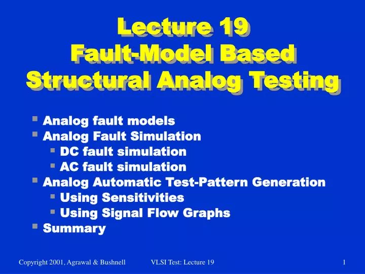
Lecture 19 Fault-Model Based Structural Analog Testing. Analog fault models Analog Fault Simulation DC fault simulation AC fault simulation Analog Automatic Test-Pattern Generation Using Sensitivities Using Signal Flow Graphs Summary. Types of Structural Faults.

E N D
Lecture 19Fault-Model Based Structural Analog Testing • Analog fault models • Analog Fault Simulation • DC fault simulation • AC fault simulation • Analog Automatic Test-Pattern Generation • Using Sensitivities • Using Signal Flow Graphs • Summary VLSI Test: Lecture 19
Types of Structural Faults • Catastrophic (hard): • Component is completely open or completely shorted • Easy to test for • Parametric (soft): • Analog R, C, L, Kn, or Kp (a transistor K parameter) is outside of its tolerance box) • Very hard to test for VLSI Test: Lecture 19
Analog Fault Models First stage gain R2 / R1 High-pass filter gain R3 and C1 High-pass filter cutoff fC1 Low-pass AC voltage gain R4, R5, & C2 Low-pass DC voltage gain R4 and R5 Low-pass filter cutoff fC2 VLSI Test: Lecture 19
Levels of Abstraction • Structural Level • Structural View – Transistor schematic • Behavioral View – System of non-linear partial differential equations for netlist • Functional Level • Structural View – Signal Flow Graph • Behavioral View – Analog network transfer function VLSI Test: Lecture 19
Analog Test Types • Specification Tests • Design characterization – Does design meet specifications? • Diagnostic – Find cause of failures • Production tests – Test large numbers of linear/mixed-signal circuits VLSI Test: Lecture 19
DC Analog Fault Simulation VLSI Test: Lecture 19
Complementarity Pivoting • P. M.Lin and Y. S. Elcherif, Analogue Circuits Fault Dictionary – New Approaches and Implementation, Int’l. J. of Circuit Theory and Applications, 1985 • Model all non-linear devices with piecewise-linear I-V characteristics (ideal diodes) • Represent open, short, and parametric faults with switches • Formulate as n-port network complementarity problem • Solve with Lemke’s complementarity pivoting algorithm • Use m pairs of complementarity variables (port currents and voltages) VLSI Test: Lecture 19
One-Step Relaxation • W. Tian and C.-J. Shi, Nonlinear DC-Fault Simulation by One-Step Relaxation – Linear Circuit Models are Sufficient for Nonlinear DC–Fault Simulation, VTS-1998 • Solve f (x) =0, x is circuit variable vector (node voltages and branch currents), f is non-linear system function • Guess x (0) • Solve Jacobian: Jf(xg) (xf(1) – xg)= -ff(xg) • Operate Newton-Raphson algorithm for only 1 step VLSI Test: Lecture 19
Fault Ordering W. Tian and C.-J. Shi, Efficient DC Fault Simulation of Nonlinear Analog Circuits, DATE-98 VLSI Test: Lecture 19
AC Fault Simulation VLSI Test: Lecture 19
Householder’s Formula • A. S. Householder, A Survey of Some Closed Methods for Inverting Matrices, SIAM J. of Applied Mathematics, 1957 • Analyze circuit with Modified Nodal Analysis: T x = w • Equivalent faulty circuit equation: Tf xf = wf • Formula (Tf differs only a little from T): (A + U S W)-1 = A-1 – A-1U (S-1 + WA-1U)-1W A-1 • Reduces amount of equation solving – 10 x speedup over sparse matrix techniques VLSI Test: Lecture 19
Discrete Z-Domain Mapping • Nagi, Chatterjee, Abraham, DRAFTS: Discretized Analog Circuit Fault Simulator, Design Automation Conference, 1993 • Analog circuit fault simulation with Signal Flow Graph (SFG) • Represented complex frequency state equations using SFGs and dummy variables • Use bilinear transform, map s-domain equations into z-domain • Accelerated fault simulation 10 times with behavioral OPAMP models VLSI Test: Lecture 19
Monte-Carlo Simulation • Perform analog simulation for randomly-generated small variations in analog circuit component values • Actual IC manufacturing makes good circuits deviate by such values • Good in practice but good and bad machines have different worst-case corners • Tends to underestimate circuit response bounds – may claim faults are detectable when they are not VLSI Test: Lecture 19
Analog Automatic Test-Pattern Generation VLSI Test: Lecture 19
Method of ATPG Using Sensitivities N. B. Hamida and B. Kaminska, Analog Circuit Testing Based on Sensitivity Computation and New Circuit Modeling, ITC-1993 • Compute analog circuit sensitivities • Construct analog circuit bipartite graph • From graph, find which O/P parameters (performances) to measure to guarantee maximal coverage of parametric faults • Determine which O/P parameters are most sensitive to faults • Evaluate test quality, add test points to complete the analog fault coverage VLSI Test: Lecture 19
Sensitivity • Differential: S = • Incremental: r =x • Tj – performance parameter • xi – network element Tj DTj / Tj D xi / xi xi Tj Tj xi xi D xi0 xi Tj DTj D xi Tj xi VLSI Test: Lecture 19
Circuit Model VLSI Test: Lecture 19
Incremental Sensitivity Matrix of Circuit -0.91 0 0 0 0 0 R1 1 0 0 0 0 0 R2 0 0.58 -0.91 0 0 0 C1 0 0.38 -0.89 0 0 0 R3 0 0 0 -0.96 -0.97 0 R4 0 0 0 0.48 -0.97 -0.88 R5 0 0 0 -0.48 0 -0.91 C2 A1 A2 fc1 A3 A4 fc2 \ VLSI Test: Lecture 19
Bipartite Graph of Circuit VLSI Test: Lecture 19
Single Fault Best and Worst-Case Deviations 5 14.81 5 15.2 5 14.65 5 13.96 5 15 5 35 5 35 DR3 R3 DC1 C1 DR5 R5 DC2 C2 DR4 R4 DR5 R5 DC2 C2 DR1 R1 DR2 R2 DR3 R3 DC1 C1 DR4 R4 DR5 R5 5 15.98 5 14.1 5 20.27 5 11.6 5 15 5 15 fc1 fc2 A3 A1 A2 A4 VLSI Test: Lecture 19
Weighted Bipartite Graph VLSI Test: Lecture 19
Analog ATPG Using Signal Flow Graphs R. Ramadoss and M. L. Bushnell, Test Generation for Mixed-Signal Devices Using Signal Flow Graphs, VLSI Design-1996 • Generates tests and defines parametric faults for analog circuits • ATPG Approach: • Backtraces signals from circuit outputs (specified with magnitude/phase tolerance) through circuit using signal flow graph (SFG) • Inverts the SFG to allow backtracing • Evaluates internal waveforms using an output waveform sample set by evaluating SFG VLSI Test: Lecture 19
Test Generation via Reverse Simulation • Find good circuit signal values at all nodes using good output waveform • Find bad circuit signal values at all nodes using bad output waveform (use extrema of tolerance box for magnitude or phase) • Finds faulty value of analog component necessary to drive output waveform out of tolerance box • Mark all corresponding edges to fault • Compute modified SFG weights that give good value after bad edges in inverted SFG VLSI Test: Lecture 19
Integrator Example • Basic integrator circuit with ideal OPAMP VLSI Test: Lecture 19
Signal Flow Graph Inversion • SFG represents analog network equations value (i) = S (parent node value) (edge weight) • May be inverted x2 = ax1 + bx3 + cx4x1 = 1/ax2 – b/ax3 - c/ax4 ORIGINAL GRAPH INVERTED GRAPH • SFG inversion algorithm follows from Balabanian’s example (1969) VLSI Test: Lecture 19
SFG Inversion Algorithm • Start at a primary input, x1, a source node • Reverse the direction of the outgoing edge from x1 to x2 and change the weight to 1/a • Redirect all edges incident on x2 to x1 and change weights appropriately • Continue for all source nodes, from all inputs, until the output becomes a source Inverted SFG Properties: • Equivalent to original SFG • A feed-forward network – graph cycles cut • Represents set of integral equations, solved by numerical differentiation • May be an unstable system VLSI Test: Lecture 19
Graphs for Integrator • SFG part after fault has faulty value • Bad signal does not disappear, circuits are linear • Method applicable to all circuits representable with SFGs (1st and 2nd order) • Backtrace over all paths from outputs to inputs • 2nd order approximation for s differential operator Inverted SFG Original SFG VLSI Test: Lecture 19
Analog Fault Definition • Want to find parametric fault value for R1 • Use good & bad node values for all nodes from reverse analog simulation • For parametric fault definition in inverted SFG • Use good values for nodes before fault • Use bad values for nodes after fault • Linear equation in 1 variable for each component • Manipulate component equations symbolically to get component tolerance VLSI Test: Lecture 19
Calculation of R1 Tolerance to Cause Fault goodval (1) badval (3) -R1 C -Rf C badval (R1) - goodval (1) C (badval (2) + badval (3) / Rf C) goodval (R1) - goodval (1) C (goodval (2) + goodval (3) / Rf C) R1Tolerance = goodval (R1) – badval (R1) Original SFG Inverted SFG + = badval (2) = = VLSI Test: Lecture 19
Component R1 Rf C Allowed Value 9.09 KW 80.99 KW 0.0093 mF Deviation -9.1% -19.01% -7.0% SFG ATPG Results • R1 = 10 KW, Rf = 100 KW, C = 0.01 mF • Output tolerance = +10%, used SPICE output • Calculated test signal and component deviations • Deviations analogous to fault coverage VLSI Test: Lecture 19
Generated Test Waveform Voltage Time (ms) VLSI Test: Lecture 19
Summary of SFG Method • Works for multiple input, multiple output circuits • Handles single and multiple parametric faults, and catastrophic faults • Symbolic solution too difficult for multiple parametric fault tolerance – use iterative method with simulation to obtain deviation • Extended to cover transistor biasing faults in analog circuits • Extended to analog multipliers and comparators VLSI Test: Lecture 19
Summary • Analog model-based testing – Just starting to get some acceptance • Structural test with a fault model • Offers advantage of testing specific parametric and catastrophic faults • Analog DSP-based testing – Main stream • Functional test without fault model • Problem is worsening – 22-bit A/D converters coming, expected to sample at 1 GHz VLSI Test: Lecture 19