Download
1 / 46
550 likes | 772 Views
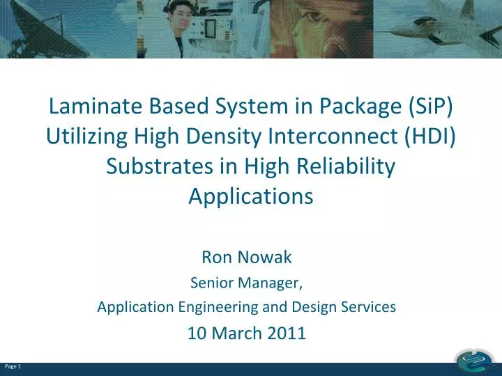
Laminate Based System in Package (SiP) Utilizing High Density Interconnect (HDI) Substrates in High Reliability Applications. Ron Nowak Senior Manager, Application Engineering and Design Services 10 March 2011. What is SiP?....An Integrated Solution. 7 mm.

E N D
Laminate Based System in Package (SiP) Utilizing High Density Interconnect (HDI) Substrates in High Reliability Applications Ron Nowak Senior Manager, Application Engineering and Design Services 10 March 2011
What is SiP?....An Integrated Solution 7 mm • System in Package (SiP) delivers 10-20X reductions from current designs • Up to 90% weight reductions • Significantly lower power and improved electrical performance • Hi-Reliability, Hi-Quality, Hi-Performance • Remove layers of interconnect • Addresses growing demand in: • Unmanned systems • Radar • Space satellites • Electronic Warfare • Medical Applications • Research Applications • The magic dust: • Bare die • HDI substrates 620mm2 PWB reduced to 30mm2
System in Package Overview • Typically multiple bare die and SMT components on a HDI microelectronics substrate: • Large and Small Bare Die placement & attach • Flip chip die connections • Wirebond die connection • Dual sided attach • Component substitution • SMT placement & attach • Down to 0201’s, 01005’s • CSP’s, SOIC’s, PLCC’s, SOJ’s • Connections to next level assembly • SMT pinned connectors • Ball Grid Array • High Density Interconnect Substrates: the secret sauce ! • Laser drilled through and microvias • 25 micron trace width and space • Thin, low loss, low dielectric constant materials
System in Package Overview • Package Size • Standard JEDEC 13.0mm to 55.0mm • Custom size and shape SiPs • Assembly to Organic Substrates • FR4 and BT epoxy • Particle filed epoxy build-up • PTFE dielectric • Kapton flex • Polyimide • LCP • Common Product Parametrics • Large MCM/SiP packages • Hybrid/double-sided assembly • Single chip module and device packages • Test • Shorts-opens • JTAG/boundary scan • Full functional test
System-in-Package Conversion • Where we begin: • Technical contact at the customer • Si design: Bare die availability • Preliminary BOM Analysis • Input • Bill of Materials & Approved Vendor List • Output • Smaller package & bare die recommendations • Preliminary Area Study • Input • Board design file & Electrical restraints • Output • initial conversion of PCB to substrate • cross section, dielectric and size estimates • Initial assembly layout • Substrate design and assembly layout • Electrical, thermal and mechanical analysis
Laminate vs. Ceramic Reliability Comparisons 45mm body size • Plastic solutions offer: • High electrical performance • High reliability performance • Weight reduction • Smaller x, y, z form factor
PTFE Substrate Chip Joining Measured flatness of 42.5mm laminate + stiffener subassembly example Viewed from BGA side: Moiré topographic fringe contours at 8.33 microns / fringe Room temperature, 20C Reflow temperature, 183C 14.7 mm size chip bump region (in red) remained flat to within 17 microns
Typical PWB to SiP Prototype Cycle Critical Design Inputs 29 weeks from design inputs to ship is common, assuming component availability BOMAnalysis BOM Substitution Recommendations SiP Physical Layout PreliminaryDesign Review SiP Physical Layout Optimization Critical Design Review Substrate Fab SiP Assembly & Test 1 week 1 week 1 week 8 weeks 2 weeks 2 weeks 2 weeks 10 weeks 2 weeks
HDI Microelectronics Packaging Menu Standard CoreEZ® HyperBGA® Microelectronics Packaging High Density Interconnect • Epoxy Glass Substrate • Cost performance • FR4, BT, Polyimide • Mechanically drilled holes • 75 micron trace • 75 micron spaces • Flip chip, Wirebond, SMT • Radiation Hard Capable • Thin Core Build Up • Cost performance • Particle filled epoxy • Thin core (coreless) • Laser drilled core • Laser drilled build up • 25 micron trace • 25 micron space • Buried resistors • Flip chip, Wirebond, SMT • Radiation Hard Capable • PTFE Substrate • High Bandwidth/RF • Particle filled material • Coreless • Laser Drilled Vias • Fusion Bonding • 25 micron trace • 33 micron space • Flip chip, Wirebond, SMT • Radiation Tolerant
Packaging Attributes applied to SiP conversions Substrate features and advanced IC Assembly techniques enable bare die implementation Flip Chip Bump 3-4-3 CoreEZ ®
Physical Design content • Physical Design Implementation • Component Placement & Routing • Physical & formal verification • Signal Integrity (SI) & Crosstalk analysis • Static Timing Analysis (STA) • Multiple Supply Voltage (MSV) • Leakage Current Reduction Techniques • Clock & Supply Voltage Gating • Power Optimization • Design for Test to ensure testability • Design for Manufacturability to maximize production yields
Signal and Power Integrity Potential Work Items and Design Flow • Typical Signal Integrity Workflow (varies by application) • Customer defines SI specifications in the form of routing constraints by net such as: • Z0 (SE, DP), Skew (Group / reference), Crosstalk / Isolation (dB @ Freq), Rdc, Insertion / Return loss (dB @ Freq), etc. • EIT ensures that these specifications are met as follows: • Pre-layout Design Guidelines: • Define stackup, function by layer, recommended component placement • Define trace width (and spacing for DP) for Z0 requirements • Translate electrical Skew requirements into physical lengths • Define spacing and coupled length limitations for crosstalk control • Define trace geometries to meet loss specification • Post-layout Verification: • Extract parameters from design database using Ansoft toolset • HFSS, Q3D, SIWave
Evaluation of Materials Subjected to Various Radiation Levels • Evaluated PTFE BGA (HyperBGA®) and Thin Core (CoreEZ®) materials radiation response • Radiation Exposure: Co60 Gamma: • Control • 32, 50, 100, 300, 500, 700, 1000 and 5000 krad TID • PTFE Materials evaluated: Rogers 2800, PPE • Results: Many applications will be unaffected by radiation • PPE has no measurable degradation to 5 Mrad • RO2800 shows gradual loss of ductility with exposure • Thin Core Build Up Materials Considered: Thermount 55LM, Particle Filled Driclad Epoxy, PSR4000 • Results: No measurable change of mechanical properties through 5 Mrad
Packaging performance after radiation exposure • Ductility performance indicates package performance in thermal cycling • Thin Core Build Up appears to be a good choice for Rad Hard and Strategic apps. • materials show no ductility degradation with radiation level • PTFE appears to be best suited for Rad Tolerant applications • PTFE ductility is higher then all other materials below 300K rad exposure • PTFE predictably degrades significantly above 300Krad exposure levels
Typical PTFE® 9 Layer Cross Section 40 micron thick APPE outer dielectric Er = 3.2 Chip Non soldermask defined pad Bump Underfill 35 micron thick PTFE Dielectric, Er = 2.7 15m thick Cu, redistribution microvia 12m thick Cu 50 micron thick PTFE Dielectric, Er = 2.7 6m Cu/38m Invar/6m Cu Ground plane 15m thick Cu, redistribution 12m thick Cu, 50m dia. through via APPE filled BGA Pad
Packaging Electrical Comparisons Notes:* measured values ; Loop inductance: Entire package , all C4 pads and BGA's commoned. The above electrical characteristics are typical of each product. Variations of these parameters can be achieved for a specific design.
PTFE Module Reliability Performance *Component w/ adhesively attached 200 gm Heat Sink on 9x10 inch card
Current Product Offering • Current Description • 4 layer, thin core (200 µm) • 50 µm UV laser drilled vias • 199 µm core pitch • Up to 4 buildup layers • Typical Cross sections: 1-4-1, 2-4-2, 3-4-3, 4-4-4 • Stacked buildup vias • 35 & 50 µm buildup thickness • 150 µm die pad pitch capable
Typical CoreEZ® 10 Layer Cross-Section Cu-filled stacked microvias Soldermask PSR4000 15 µm thick Flip Chip Bumps GND / TOP Build-up layer 1 Build-up layer 2 Build-up layer 3 Driclad, 35/50 µm thick S1 PWR / GND S2 Outer core Dielectric, Driclad 35/50 µm thick PWR / GND Inner core 135 µm thick Epoxy/P-Aramid PWR / GND Core Cu 12 µm thick S3 PWR / GND Build-up Cu 1 Build-up Cu 2 Build-up Cu 3 12 µm thick S4 GND / BOT • 3-4-3 Stack up (10 copper layers) • Substrate thickness 0.7 mm
8 Layer X-Section Comparison CoreEZ® 2-4-2 Standard Build-up 3-2-3 Photographs are at same magnification - Both packages use 50um blind vias - CoreEZ® core vias are 4x smaller - Enhanced high speed electrical performance
HDI With High Core Via Density • Dense Package Interconnect • Dense Core Via Pitch • Dual Side Component Mounting • Fine Line Width and Spacing • Enhanced Z-axis connectivity Thin Core, SiP 50 um via Standard Build-Up 500 um via ~9X Core Via Density
CoreEZ™ Typical X-Sections • CoreEZ™ is available as a 1-4-1, 2-4-2 , 3-4-3 or 4-4-4 cross sections • 1-4-1 = 2 full stripline signal planes, 4 pwr/gnd • 2-4-2 = 4 dual stripline signal planes, 4 pwr/gnd • 3-4-3 = 4 full stripline signal planes, 6 power/gnd • 4-4-4 = 4 full stripline signal planes, 8 pwr/gnd 4 – 4 - 4
Embedded Passives in CoreEZ® • Resistors • Thin film resistor material • Ticer TCR® • 10 - 250 ohms per square • Resistor values from 5 ohm to 50 Kohm • Resistor tolerances from 2 – 20% • Laser trimming 2 – 5% • Typical resistor areas • 0.2 – 15 mm2 • Block or Serpentine designs Eight layer core 285 nF / in2
300 mV 43 ps High Speed SERDES in CoreEZ®Simulation at 12.5 Gbps • Similar electrical performance as PTFE • Within 10% of PTFE jitter performance
Why LCP? • Is “near” hermetic • Low moisture absorption: 0.04% • Halogen Free (lead free assembly being evaluated) • Similar in electrical performance to PTFE • Low Loss • Dk = 2.9 • Df = 0.0025 • Very Lightweight • 1.4gm/cm3 • Thermoplastic • Thin and thick layer combinations in cross sections • 25um, 50 um and 100 um thickness • Capable of Radiation Hardened applications • Rogers ULTRALAM 3850, 3908 • Nippon Steel Espanex L
4-Layer LCP x-sections: 100 um LCP 50 um LCP 100 um LCP • 50 micron laser thru vias • 50 micron buried vias • 50 micron thick LCP • 100 micron thick LCP • 37.5 micron LW & Space • Staggered Blind Vias • Rogers Ultralam 3850, 3908 50 um 50 um 50 um
First level Assembly Overview Electronic packaging development, fabrication and advanced assembly of complex flip chip and wire bond packages • Key differentiators: • Flip Chip, Wirebonding and SMT on one package • BGA balling • Lead-free assembly • 01005 component placement and assembly • Alternative pad finishes • Teradyne Ultra FLEX VLSI platform functional testing • Leading edge process development
First level Assembly-Wirebond • Wire Bond Expertise…… • Die-up and cavity • Ball bonding 25 micron diameter Au wire to 125 micron pitch • Pitches down to 57µm on 700+ wire package • Production qualified for military applications • Die attach: sizes to 16mm square • Ribbon bonding packages and cards to 12” • Al ribbon bonding available • Coplanarity measurements • Damming and glob top
Flip Chip Assembly Needs • Flip Chip Expertise • SiGe, Si, GaAs die attach • Hi melt, eutectic, Sn cap C4, Pb-free • Low alpha Sn/Pb solder • High I/O Flip Chip join down to 150µm pitch • Die sizes placed to 25mm x 26mm • Flux chemistries/dispensing • Various low & high modulus underfills • BGA attach down to 0.5mm pitch (eutectic, Pb-free) • PGA attach • Thermal adhesive • Heat spreader, heat sink & lid attach • 100µm pitch solder dispense • Solder volume measurements • CSAM acoustic imaging inspection • X-ray inspection • Part labeling/marking: traceability
Assembly Engineering Support Support Operations • Pre/post assembly coplanarity measurement • Acoustic microscopy for interfacial inspection • Real time X-ray for process monitors • Ionic cleanliness measurements • Wire pull and ball shear • Solder repair/rework • Cross section support failure analysis • Traceability to the component level • Fixturing and process development AIR-VAC Hot Air Rework Tool • Can rework leaded, lead free, and high melt BGA’s, Micro BGA’s, and flip chip die.
Extreme SiP Miniturization example Original PCB 620 mm2 • Package Size • 30 mm diameter, 391 total components • 39 different part numbers, 231 components on 2 surfaces • 5 Bare Die • Flip Chip FPGA, 15.95mm x 10.23mm, 2,440 I/O • Flip Chip DSP, 4.68mm x 5.134mm, 225 um pitch, 261I/O • Flip Chip Supply monitor, pitch = 114 um, 16 I/O • Flip Chip DRAM, pitch = 121 um, 86 i/o • Flip Chip Flash memory, pitch = 116 um, 77 I/O • 178 SMT Capacitors, 14 SMT resistors • 152 buried resistors imbedded in substrate • 1 SMT circular connector • > 100 produced SiP CoreEZTM30 mm2
Intravascular Ultrasound Catheter Sensor Package Transducer ASIC Die 7 mm Single layer HDI Flex • Flip Chip Ultrasound Transducer for Catheter • sensor assembly rolled to 1.175mm diameter • 5 Flip Chip ASIC,.1mm thick, 31 I/O, 2.5mm x .5mm • 22 micron flip chip bumps on 70 micron die pad pitch • 1 PZT crystal • 12.5mm by 6.5 mm single layer flex circuit • 14 micron wide lines and space copper circuitry • 12.5 thick polyimide dielectric • Prototype to production • Over 320,000 modules shipped Flip Chip Bumps 200 µm
Low Level Gamma Photon Detector Module • 9 layer HyperBGA PTFE Substrate • Bottom side CZT Crystal • Passives on mini card • S. Steel Stiffener • Top side Wirebonded ASIC • 50 micron UV laser drilled vias • 25 micron trace • 33 micron space Hyper Substrate X-Section Substrate Top Substrate Bottom ASIC site CZT site
Microelectronics Packaging Conclusion Enable System Miniaturization using SiP: Bare die, HDI Substrate Materials, Assembly Technology & Manufacturing • Combining advanced flip chip & wirebond with maximum HDI plastic substrates • Deliver maximum reliability and electrical performance for RF and High Bandwidth Digital • System Level Shrink for SWaP • PWB redesigns into fully integrated System in Package • 24X system size reductions have been realized • Lower cost next level assemblies (lower layer count PWB’s) Deliver the industry’s smallest packages combined with superior package reliability and robust electrical performance!
Acknowledgments • The author would like to thank CERN for their invitation to participate in the ACES Workshop in Geneva and also thank the CEO of Endicott Interconnect Technologies for his kind permission to present this paper. • Ron Nowak • Email: ron.nowak@eitny.com • Web site: www.endicottinterconnect.com