Download
1 / 39
420 likes | 785 Views
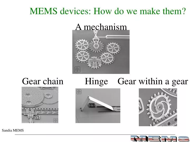
MEMS devices: How do we make them?. A mechanism. Gear chain Hinge Gear within a gear. Sandia MEMS. Basic MEMS materials Silicon and its derivatives, mostly. Micro-electronics heritage Si is a good semiconductor, properties can be tuned Si oxide is very robust

E N D
MEMS devices: How do we make them? A mechanism Gear chain Hinge Gear within a gear Sandia MEMS
Basic MEMS materials Silicon and its derivatives, mostly • Micro-electronics heritage • Si is a good semiconductor, properties can be tuned • Si oxide is very robust • Si nitride is a good electrical insulator
Surface micromachining How a cantilever is made: http://www.darpa.mil/mto/mems
One can make devices as complex as one wishes using deposition and micromachining processes http://mems.sandia.gov/
Any MEMS device is made from the processes of deposition and removal of material e.g. a state-of-the art MEMS electric motor www.cronos.com
The History of MEMS Y.C.Tai, Caltech
Bulk micromachining • Wet Chemical etching: Masking layer Bulk Si Bulk Si Isotropic Anisotropic
Bulk micromachining • Dry etching • Ions: Reactive ion etching (RIE), focused ion beams (FIB) • Laser drilling: using high powered lasers (CO2/YAG) • Electron-beam machining: sequential slow
Wet Etching: Isotropic • atomic layer by atomic layer removal possible • Isotropic etching:Hydrofluoric + nitric + acetic acids (HNA) Bulk Si Chemical reaction: Si + 6 HNO3+6 HF H2SiF6 + HNO2 + H2O + H2 Principle: HNO3 (Nitric acid) oxidizes Si SiOx HF (Hydrofluoric Acid) dissolves SiOx Acetic acid/water is a diluent
Z Y X Anisotropic etching, due to the Silicon crystal structure - Diamond cubic crystal structure Different planes of atoms in a Silicon crystal have different densities of atoms (111) (100) (110) (111) This implies preferential/anisotropic etching is possible
fiber Applications: Anisotropic Etching Inkjet printers Aligning fibers
Wet etching: Anisotropic Etching (100) (110) (100) (111) Bulk Si Bulk Si Chemical recipes: EDP (Ethylene diamine, pyrocatechol, water) [NH2(CH2)2NH2, C6H4(OH)2] - low SiO2 etch rate, - carcinogenic KOH (Potassium hydroxide), - high <110> / <111> and <100>/ <111> selectivity ( ~ 500) - high SiO2 etching TMAH (Tetra-methyl Ammonium Hydroxide: (CH3)4NOH) - Low SiO2 and SixNy etch rate - smaller <100> / <111> selectivity
Comparison of wet chemical etches Reference: “Etch rates for Micromachining Processing” - K. R. Williams, IEEE Journal of MEMS, vol. 5, page 256, 1996.
Sensors based on (100) preferential etching Honeywell sensor
Micro-fluidic channels based on (110) preferential etching
MEMS Process Sequence Slide courtesy: Al Pisano
Surface micromachining How a cantilever is made: http://www.darpa.mil/mto/mems Sacrificial material: Silicon oxide Structural material: polycrystalline Si (poly-Si) Isolating material (electrical/thermal):Silicon Nitride
MEMS Processing Oxidation of Silicon Silicon Oxide (Sacrificial material) Dry Oxidation: flowing pure oxygen over Si @ 850 – 1100 oC (thin oxides 1- 100 nm, high quality of oxide) Uses the Deal-Grove Model: xoxide = (BDGt)1/2 Temperature (oC)BDG (mm2/ hour) 920 0.0049 1000 0.0117 1100 0.027
MEMS Processing Oxidation of Silicon Silicon Oxide (Sacrificial material) Wet Oxidation: uses steam for thicker oxides (100nm – 1.5 mm, lower quality) Temperature (oC)BDG (mm2/ hour) 920 0.203 1000 0.287 1100 0.510 Higher thicknesses of oxide: CVD or high pressure steam oxidation
Silicon oxide deposition SiH4 + O2 LTO: Low Temperature Oxidation process • For deposition at lower temperatures, use • Low Pressure Chemical Vapor Deposition (LPCVD) • SiH4 + O2 SiO2 + 2H2 : 450 oC • Other advantages: • Can dope Silicon oxide to create PSG (phospho-silicate glass) • SiH4 + 7/2 O2 + 2 PH3 SiO2:P + 5 H2O : 700 oC • PSG: higher etch rate, flows easier (better topography) 425-450 oC 0.2-0.4 Torr
Case study: Poly-silicon growth SiH4 Amorphous film 570 oC Crystalline film 620 oC • by Low Pressure Chemical Vapor Deposition • T: 580-650 oC, P: 0.1-0.4 Torr • Effect of temperature • Amorphous Crystalline: 570 oC • Equi-axed grains: 600 oC • Columnar grains: 625 oC • (110) crystal orientation: 600 – 650 oC • (100) crystal orientation: 650 – 700 oC Kamins,T. 1998 Poly-Si for ICs and diplays, 1998
Poly-silicon growth • Temperature has to be very accurately controlled • as grains grow with temperature, increasing surface • roughness, causing loss of pattern resolution and stresses in • MEMS • Mechanisms of grain growth: • Strain induced growth • - Minimize strain energy due to mechanical deformation, doping … • - Grain growth time • 2. Grain boundary growth • - To reduce surface energy (and grain boundary area) • - Grain growth (time)1/2 • 3. Impurity drag • - Can accelerate/prevent grain boundary movement • - Grain growth (time)1/3
Grains control properties • Mechanical properties • Stress state:Residual compressive stress (500MPa) • - Amorphous/columnar grained structures: Compressive stress • - Equiaxed grained structures: Tensile stress • Thick films have less stress than thinner films • ANNEALING CAN REDUCE STRESSES BY A • FACTOR OF 10-100 • Thermal and electrical properties • Grain boundaries are a barrier for electrons • e.g. thermal conductivity could be 5-10 times lower (0.2 W/cm-K) • Optical properties • Rough surfaces!
Silicon Nitride SiH2Cl2 + NH3 (for electrical and thermal isolation of devices) r: 1016W cm, Ebreakdown: 107 kV/cm • Is also used for encapsulation and packaging • Used as an etch mask, resistant to chemical attack • High mechanical strength (260-330 GPa) for SixNy, provides structural integrity (membranes in pressure sensors) • Deposited by LPCVD or Plasma –enhanced CVD (PECVD) LPCVD: Less defective Silicon Nitride films PECVD: Stress-free Silicon Nitride films x SiH2Cl2 + y NH3 SixNy + HCl + 3 H2 700 - 900 oC 0.2-0.5 Torr
Depositing materialsPVD (Physical vapor deposition) • Sputtering: DC (conducting films: Silicon nitride) RF (Insulating films: Silicon oxide) http://web.kth.se/fakulteter/TFY/cmp/research/sputtering/sputtering.html
Depositing materialsPVD (Physical vapor deposition) • Evaporation (electron-beam/thermal) Commercial electron-beam evaporator (ITL, UCSD)
Electroplating Courtesy: Jack Judy • Issues: • Micro-void formation • Roughness on top surfaces • Uneven deposition speeds • Used extensively for LIGA processing e.g. can be used to form porous Silicon, used for sensors due to the large surface to volume ratio
Depositing materials –contd.- • Spin-on (sol-gel) • e.g. Spin-on-Glass (SOG) used as a sacrificial molding material, processing can be done at low temperatures Dropper Si wafer
Surface micromachining - Technique and issues - Dry etching (DRIE) Other MEMS fabrication techniques - Micro-molding - LIGA Other materials in MEMS - SiC, diamond, piezo-electrics, magnetic materials, shape memory alloys … MEMS foundry processes - How to make a micro-motor
Surface micromachining Carving of layers put down sequentially on the substrate by using selective etching of sacrificial thin films to form free-standing/completely released thin-film microstructures http://www.darpa.mil/mto/mems HF can etch Silicon oxide but does not affect Silicon Release step crucial
Release of MEMS structures • A difficult step, due to surface tension forces: Surface Tension forces are greater than gravitational forces ( L) ( L)3
Cantilever Si substrate Release of MEMS structures • To overcome this problem: • Use of alcohols/ethers, which sublimate, at release step • Surface texturing • Supercritical CO2 drying: avoids the liquid phase 35oC, 1100 psi
A comparison of conventional vs. supercritical drying
Reactive Ion Etching (RIE) DRY plasma based etching http://www.memsguide.com • Deep RIE (DRIE): • Excellent selectivity to mask material (30:1) • Moderate etch rate (1-10 mm/minute) • High aspect ratio (10:1), large etch depths possible
Deep Reactive Ion Etching (DRIE) A side effect of a glow discharge polymeric species created Plasma processes: Deposition of polymeric material from plasma vs. removal of material Usual etching processes result in a V-shaped profile Bosch ProcessAlternate etching (SF6) +Passivation (C4F8) • Bowing: bottom is wider • Lag: uneven formation
Gas phase Silicon etching • Room temperature process • No surface tension forces • No charging effects • Isotropic XeF2 BrF3 Developed at IBM (1962) Developed at Bell labs (1984) 2 XeF2 + Si 2 Xe + SiF4 4 BrF3 + 3 Si 2 Br2 + 3 SiF4 Cost: $150 to etch 1 g of Si $16 for 1 g of Si Etching rate: 1-10 mm/minute
Micro-molding • For thick films (> 100 mm) • HEXSIL/PDMS, compatible with Bio-MEMS C. Keller et al, Solid state sensor & actuator workshop, 1994 - loss of feature definition after repeated replication - Thermal and mechanical stability
LIGA (LIthographie, Galvanoformung, Abformung) • For high aspect ratio structures • Thick resists (> 1 mm) • high –energy x-ray lithography ( > 1 GeV) • Millimeter/sub-mm sized objects which require precision Mass spectrometer with hyperbolic arms Electromagnetic motor
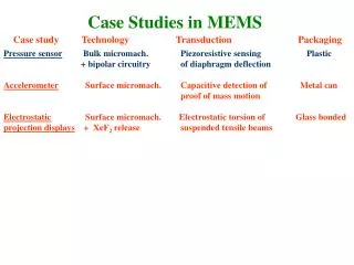
Technology Comparison Bulk vs. Surface micromachining vs. LIGA