Download
1 / 14
180 likes | 575 Views
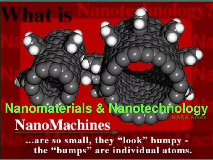
Nanomaterials & Nanotechnology. What does “Nano” mean?. Nano (Greek): dwarf Nano(technology) refers to particle sizes at nano-scale : 1 nm = 10 –9 m = 0.000,000,001 m Comparison of 1 m with 1 nm equals approximately the size of the earth compared with the size of dice. vs.

E N D
What does “Nano” mean? • Nano (Greek): dwarf • Nano(technology) refers to particle sizes at nano-scale: 1 nm = 10–9 m = 0.000,000,001 m • Comparison of 1 m with 1 nm equals approximately the size of the earth compared with the size of dice vs.
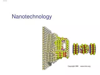
The Nanometer Size Scale Nanotube
A Brief History The history of nanotechnology reaches back to the late 19th century, when colloidal science first took root. The first mention of some of the distinguishing concepts in nano-technology was in “There’s Plenty of Room at the Bottom”, a talk given by physicist Richard Feynman at an APS meeting in 1959. The term “nanotechnology” was defined by Prof. N. Taniguchi (“On the Basic Concept of ‘Nano-Technology’,” Proc. Intl. Conf. Prod. Eng. Tokyo, Part II, JSPE, 1974.) as follows: “‘Nano-technology’ mainly consists of the processing of, separation, consolidation, and deformation of materials by one atom or one molecule.” In the 1980s the basic idea of this definition was explored in much more depth by Dr. K. E. Drexler, who promoted the technological significance of nanoscale phenomena and devices through speeches and books.
Nanotechnology and nanoscience got started in the early 1980s with two major developments: the birth of cluster science and the invention of the scanning tunneling microscope (STM). This development led to the discovery of fullerenes and carbon nanotubes. The synthesis and properties of semiconductor nanocrystals were studied. This led to a fast increasing number of metal oxide nanoparticles of quantum dots (QDs).
A QD is a semiconductor nanostructure that confines the motion of conduction band electrons, valence band holes, or excitons (pairs of conduction band electrons and valence band holes) in all three spatial directions. The confinement can be due to (1) electrostatic potentials (generated by external electrodes, doping, strain, impurities), (2) the presence of an interface between different semiconductor materials (e.g., in the case of self-assembled quantum dots), (3) the presence of the semi-conductor surface (e.g., in the case of a semiconductor nanocrystal), or (4) a combination of these. A QD has a discrete quantized energy spectrum. The corresponding wave functions are spatially localized within the QD but extend over many periods of the crystal lattice.
QDs can be contrasted to other semiconductor nanostructures: 1) quantum wires, which confine the motion of electrons or holes in two spatial directions and allow free propagation in the third; 2) quantum wells, which confine the motion of electrons or holes in one direction and allow free propagation in two directions. In contrast to atoms, the energy spectrum of a QD can be engineered by controlling the geometrical size, shape, and the strength of the confinement potential. In QDs that confine e– and h+, the interband absorption edge is blue shifted due to the confinement compared to the bulk material of the host semiconductor material. As a consequence, QDs of the same material, but with different sizes, can emit light of different colors.
The larger the dot, the redder the fluorescence; the smaller the dot, the bluer it is. Quantitatively speaking, the band gap that determines the energy (and hence color) of the fluoresced light is inversely proportional to the square of the size of the quantum dot. Larger QDs have more energy levels which are more closely spaced. This allows the QD to absorb photons containing less energy, i.e. those closer to the red end of the spectrum. The ability to tune the size of QDs is advantageous, as the larger and more red-shifted the QDs, the less the quantum properties are. The small size of the QD allows people to take advantage of these quantum properties.