Download
1 / 23
230 likes | 371 Views
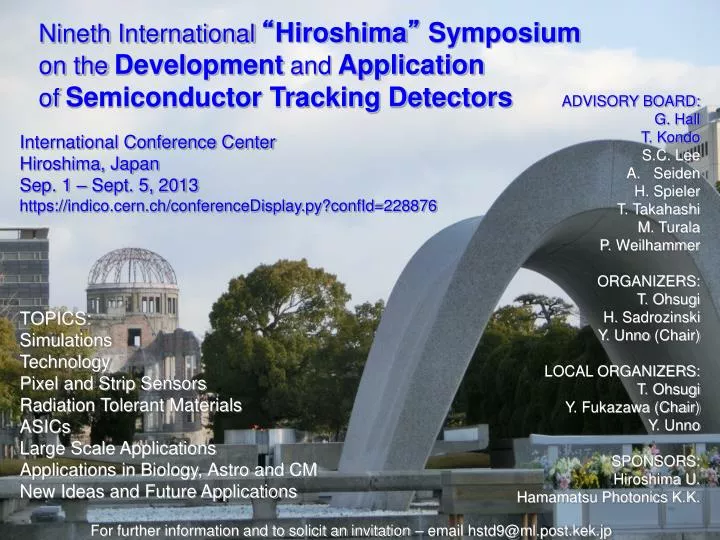
Nineth International “ Hiroshima ” Symposium on the Development and Application of Semiconductor Tracking Detectors. ADVISORY BOARD: G. Hall T. Kondo S.C. Lee Seiden H. Spieler T. Takahashi M. Turala P. Weilhammer ORGANIZERS: T. Ohsugi H. Sadrozinski Y. Unno (Chair)

E N D
Nineth International“Hiroshima” Symposium on theDevelopmentandApplication ofSemiconductor Tracking Detectors • ADVISORY BOARD: • G. Hall • T. Kondo • S.C. Lee • Seiden • H. Spieler • T. Takahashi • M. Turala • P. Weilhammer • ORGANIZERS: • T. Ohsugi • H. Sadrozinski • Y. Unno (Chair) • LOCAL ORGANIZERS: • T. Ohsugi • Y. Fukazawa (Chair) • Y. Unno • SPONSORS: • Hiroshima U. • Hamamatsu Photonics K.K. International Conference Center Hiroshima, Japan Sep. 1 – Sept. 5, 2013 https://indico.cern.ch/conferenceDisplay.py?confId=228876 TOPICS: Simulations Technology Pixel and Strip Sensors Radiation Tolerant Materials ASICs Large Scale Applications Applications in Biology, Astro and CM New Ideas and Future Applications For further information and to solicit an invitation – email hstd9@ml.post.kek.jp
Scribe-Cleave-Passivate (SCP) Slim Edge Technologyfor Silicon Sensors Scott Ely, Colin Parker, Jeffrey Ngo, VitaliyFadeyev, Hartmut F.-W. Sadrozinski Santa Cruz Institute for Particle Physics, University of California Santa Cruz TREDI 2013 Hartmut Sadrozinski, SCP Slim Edge Technology for Silicon Sensors
Outline • S-C-P of full-size sensors for proton CT • S-C-P Slim Edges – p-type vs. n-type • Irradiations with protons • S-C only: no passivation • S-C-P p-type CIS • S-C-P p-type and n-type HPK • Guidance and Technical Support by • Marc Christophersen, Bernard F. Phlips • Code 7654, U.S. Naval Research Laboratory TREDI 2013 Hartmut Sadrozinski, SCP Slim Edge Technology for Silicon Sensors
Large area coverage requires tiling of 4 sensors, having ~ 1mm inactive edges which create image artifacts. Overlapping sensors introduces artifacts requiring additional, non-uniform energy corrections S-C-P treated SSD in pCT Tracker For Tiling with no Overlap: “Slim Edges” Si SSD with 900mm dead edge Cut within 50 mm of Guard Ring with guard ring S-C-P: Scribing (XeF2) + Cleaving + Passivating (N2 PECVD) M. Christophersen et al., SSE 81, (2013) 8–12 TREDI 2013 Hartmut Sadrozinski, SCP Slim Edge Technology for Silicon Sensors
S-C-P treated 9 cm x 9 cm HPK SSD (ex GLAST) • Cut 2 opposing edges only • Observe considerable annealing effects! TREDI 2013 Hartmut Sadrozinski, SCP Slim Edge Technology for Silicon Sensors
Slim Edges -- Motivation Basic Idea: To minimize ~1 mm wide inactive peripheral region. This is relevant for “tiling” (as opposed to “shingling”) of large-area detector composed of small sensors. Basic Method: To instrument the sidewall in a close proximity to active area, such that it’s resistive. TREDI 2013 Hartmut Sadrozinski, SCP Slim Edge Technology for Silicon Sensors
Method -- SCP Treatment Scribing Cleaving Passivation finished die with slim edge finished die finished die • Native Oxide • + Radiation • or: • N-typeP-type • Native SiO2 • + UV light • or high T • PECVD SiO2 • PECVD Si3N4 • ALD “nanostack” • of SiO2 and Al2O3 • Diamond stylus • Laser • XeF2 Etch • DRIE Etch • Tweezers (manual) • Loomis Industries, LSD-100 • Dynatex, GTS-150 • ALD • of Al2O3 All Treatment is post-processing & low-temp (Etch-scribing can be done during fabrication) Basic requirement: 100 wafers (for rectangular side cleaving) with reasonably good alignment between sensor and lattice. TREDI 2013 Hartmut Sadrozinski, SCP Slim Edge Technology for Silicon Sensors
Passivation Options • Surface passivation makes the sidewall resistive. N- and p-type devices require different technologies. • For n-type devices one needs a passivation with positive interface charge. SiO2 and Si3N4 layers works well. • For p-type material a passivation with negative interface charge is necessary. We found that Al2O3 works in this case. TREDI 2013 Hartmut Sadrozinski, SCP Slim Edge Technology for Silicon Sensors
SCP Treatment (Cont) finished die laser-, diamond-, or etch-scribing cleaving This is an optional step for the SCP process. A gaseous Xenon Difluoride (XeF2) etch step can remove scribing damage: needed for Laser and diamond scribe). XeF2 etch step annealing and testing sidewall passivation TREDI 2013 Hartmut Sadrozinski, SCP Slim Edge Technology for Silicon Sensors
Scribing Technologies: Diamond-, Laser-, and Etch-based Diamond scribing Laser scribing • Issues: • Diamond scribing: surface chipping of existing passivation (=> to do again in future runs) • Laser scribing: some degree of damage due to affected region of the sidewall • XeF2etching: cleaving by industrial machines is difficult TREDI 2013 Hartmut Sadrozinski, SCP Slim Edge Technology for Silicon Sensors
Scribing Technologies: DRIE • litho step • open oxide with Vapox III Etch (wet etch) • DRIE etch • laser-scribing • cleaving using tweezers • XeF2 sidewall etch (5 cycles) • H-termination of sidewall (wet etch) • ALD deposition, SiO2 and Al2O3 • Anneal @ 400 degree C for 10 min DRIE-based trenching as scribing has a promised of being a “universal” production solution without shortcomings of the other methods. TREDI 2013 Hartmut Sadrozinski, SCP Slim Edge Technology for Silicon Sensors
Al2O3 Al2O3 Al2O3 Effect of Surface Termination – P-Type Si HPK ATLAS07 P-Type Diodes • After all the handling, we need to remove a native oxide. That is done w/ HF and leads to the “H-termination”, which can’t be passivated with alumina Al2O3. • Need to covert the H-termination into F-termination which in combination with alumina ALD should work. Know they chemistry! • The hunt for on ideal surface termination for p-type Si is still on. TREDI 2013 Hartmut Sadrozinski, SCP Slim Edge Technology for Silicon Sensors
Progress with Passivation (N-type Diodes) PECVD process has been developed by industry as a wafer process => Small height of the chamber in a typical machine. This worked well for small size samples, that could be positioned vertically, or slanted. For large sensors this is not quite applicable => replace by ALD method. Study with HPK Fermi/GLAST diodes. The plain ALD SiO2 is worse than the best case of PECVD Si3N4. But a “nanostack” of ALD SiO2 (10 nm) and Al2O3 (50 nm) works well.Parameters are from G. Dingemans et al, J. Appl. Phys. 110, 093715 (2011); doi: 10.1063/1.3658246 Consistently low I and high B(break). Quite similar to the best case of PECVD nitride! TREDI 2013 Hartmut Sadrozinski, SCP Slim Edge Technology for Silicon Sensors
1. 2010 Proton Irradiation Studies @LANL • S-C only: No Passivation P-type HPK (ATLAS07) These are sensors which did not work after cleaving (at the time we did not realize the importance of the proper surface charge). Breakdown at ~few Volts. There is an empirical evidence that the breakdown improves after irradiation. We put these sensors in proton beam to see if they would indeed improve • Observation #1 on S-C only p-type: • High fluence irradiation -> high resistivity bulk -> edge isolation! TREDI 2013 Hartmut Sadrozinski, SCP Slim Edge Technology for Silicon Sensors
2. 2011 Proton Irradiation @LANL • Irradiated 12 SCP processed p-type strip devices (CIS courtesy A. Macchiolo) at LANL (thanks S. Seidel) • Results are in-conclusive: + Breakdown voltages extended post-rad + High fluence devices (3/3 for 1e16neq, 3/3 for 1e15neq) show expected post-rad leakage current - Lower fluence devices (1/3 for 1e13neq and 1/3 for 1e14neq) show very early breakdown!!! A parallel investigation of the robustness of the passivation layer revealed a possible susceptibility to rough handling. There is no proof that this has skewed the irradiation results. TREDI 2013 Hartmut Sadrozinski, SCP Slim Edge Technology for Silicon Sensors
2. 2011 Proton Irradiation @LANL • Observation #2 on S-C-P p-type: • Low fluence (< 1e15): no edge-isolation • High fluence irradiation (< 1e15 ?): edge isolation! TREDI 2013 Hartmut Sadrozinski, SCP Slim Edge Technology for Silicon Sensors
3. 2012 Proton Irradiation @CERN • A round of irradiations at SPS (help from G. Casse & M. Glaser): • p-type diodes from ATLAS07 Test Structures • n-type diodes from Fermi/GLAST Test Structures, with both PECVD nitride and ALD oxide PPS Meeting, June 14-15, 2012 Progress on SCP Slim Edge Technology 17 TREDI 2013 Hartmut Sadrozinski, SCP Slim Edge Technology for Silicon Sensors
n-type GLAST HPK Photo Diodes both nitrite and oxide passivation Expected current [uA] @ -5 C 13.3 1.33 0.16 PRELIMINARY Pre-rad Oxide Nitrite • Observation #3 on S-C-P n-type: • No dependence on type of passivation, leakage current close to bulk expectation • low fluence(1e13, below inversion) edge isolation due to Oxide/Nitrite • High fluence (>1e14, after inversion): edge isolation due to bulk resistivity TREDI 2013 Hartmut Sadrozinski, SCP Slim Edge Technology for Silicon Sensors
p-type ATLAS07 HPK Photo Diodes Expected current [uA] @ -5 C 8 0.8 0.1 PRELIMINARY Pre-rad • Observation #4 on S-C-P p-type: • Leakage currents do not scale with fluence • low fluence(< 1e14): reduced effect of Alumina ALD edge isolation • high fluence (>1e14): edge isolation works due to increased bulk resistivity TREDI 2013 Hartmut Sadrozinski, SCP Slim Edge Technology for Silicon Sensors
Conclusions and Future Work • We have started S-C-P treatment of full-size 6” HPK n-type sensors • After 3 irradiations we start to be able to interpret the observed post-radiation behaviour in terms of • an increased bulk resistivity improving the edge isolation, • and a potential reduction of the edge isolation created by the passivation due to type inversion (n-type) and an apparent growing in-effectiveness of the alumina ALD (p-type). • In order to really understand the root cause for the performance, we will perform the following studies: • Annealing • Temperature dependence • Neutron irradiation (reduce the influence of interface charges, bulk effects only) • Gamma irradiation (reduce bulk effects, increase interface charge effects) TREDI 2013 Hartmut Sadrozinski, SCP Slim Edge Technology for Silicon Sensors
Acknowledgements Members of RD50 and ATLAS Upgrade for supplying sensors. GianluigiCasse, Vladimir Cindro, Maurice Glasser, Sally Seidel for Irradiations. TREDI 2013 Hartmut Sadrozinski, SCP Slim Edge Technology for Silicon Sensors
Back-Up Slides TREDI 2013 Hartmut Sadrozinski, SCP Slim Edge Technology for Silicon Sensors
Charge Collection Testing TREDI 2013 Hartmut Sadrozinski, SCP Slim Edge Technology for Silicon Sensors