Download
1 / 9
160 likes | 400 Views
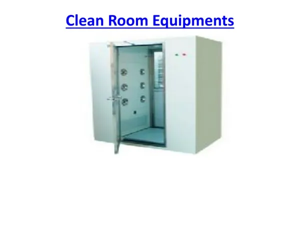
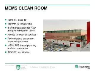
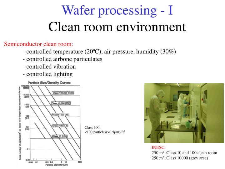
Wafer processing - I Clean room environment. Semiconductor clean room: - controlled temperature (20ºC), air pressure, humidity (30%) - controlled airbone particulates - controlled vibration - controlled lighting. Class 100: <100 particles(>0.5 m m)/ft 3. INESC:

E N D
Wafer processing - IClean room environment Semiconductor clean room: - controlled temperature (20ºC), air pressure, humidity (30%) - controlled airbone particulates - controlled vibration - controlled lighting Class 100: <100 particles(>0.5mm)/ft3 INESC: 250 m2 Class 10 and 100 clean room 250 m2 Class 10000 (grey area)
Wafer processing - IIresist coating 1- Vapor priming for improved resist adhesion to substrate • - Resist adhesion to Si wafers is poor • Dehydration bake to remove adsorbed water from the surface • surfactant to promote adhesion : HMDS (hexamethyldisilazane) Vapor priming is better than spin coating with a liquid solution because lower contamination ~1 monolayer
Wafer processing - IIresist coating 2- Spinning resist and soft baking Requirements: Good control of thickness, uniformity, viscosity, particle contamination Typical resist thickness: 0.6-2 mm Soft baking: remove solvents and stress and promote adhesion to wafer SVG Resist coater and developer track: Track system for spin coating of photoresist (1.2 to 2 mm thick) and for development of post-exposed wafers. (cassettes of 25 Si wafers F6 inch)
Coating and developing Exposure (c) F6 inch Si wafers Wafer processing - II
Wafer processing - IIIexposure INESC Heidelberg Instruments Direct Write Laser Lithography System: Direct write lithography system utilizing a HeCd laser (l=442 nm (g-line) / write lens NA= 0.85) capable of critical dimensions down to 0.8 mm. System works with mask designs in GDS2 format.
Wafer processing - IVdevelopment Selective dissolving of resist (INESC) Positive resists Negative resists Remain in the exposed regions Solved in the exposed regions