Download
1 / 22
250 likes | 355 Views
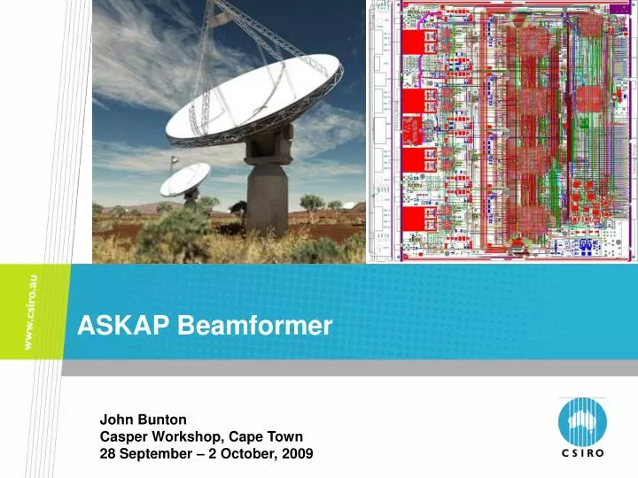
ASKAP Beamformer. John Bunton Casper Workshop, Cape Town 28 September – 2 October, 2009. The Task. 36 antennas with 94 dual pol feeds + 4 calibration/RFI signals (192 total) 304Mhz from each feed (BW/antenna 60GHz = ATA 100MHz)

E N D
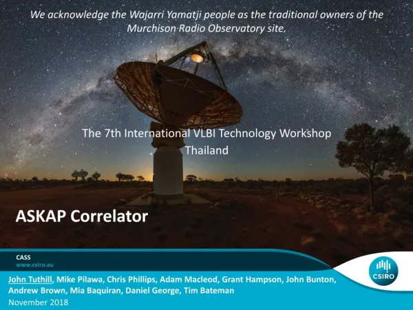
ASKAP Beamformer John Bunton Casper Workshop, Cape Town 28 September – 2 October, 2009
The Task • 36 antennas with 94 dual pol feeds + 4 calibration/RFI signals (192 total) • 304Mhz from each feed (BW/antenna 60GHz = ATA 100MHz) • Beamform data for each antenna to generate up to 36 dual pol beams • Generate 18.5kHz frequency channels across 304MHz • Full Stokes FX correlator • Compute requirements over 1015 op/s • Also • Min 32 tied array beams for Pulsar • 4 beams at VLBI clock rate • 8MHz with 0.5kHz channels • … • Implemented in FPGA • Objective – minimise cost and power (~$4W/year)
Progress • First antenna - acceptance testing • First installation Boolardy – November 2009 • Field testing of 40 element Phased Array Feed • Digital system Engineering System 1 • Virtex 5 • Hardware complete • ADC, coarse filterbank, signal transport - final testing • Digital systems Critical Design Review 20 October • About to start work on Engineering system 2 • Virtex 6 • Mid 2010 two complete antennas with PAFs, ES2 Beamformers and Correlator
The Team • John Bunton Project Leader • Grant Hampson Project Engineer • Ilana Feain Project Scientist • Alan Ng Project Manager • Paul Roberts ADC • Joseph Pathikulangara Hardware/Firmware • John Tuthill Hardware/Firmware • Andrew Brown Hardware/Firmware • Jayasri Joseph Firmware • Tim Bateman Firmware • Ludi de Souza Firmware • Evan Davis Control PC's and Networks • Ron Koenig Parts and Library manager • Matt Shield Hardware Assembly / Testing • Raji Chekkala Hardware Assembly • Troy Elton Mechanical • Other projects Signal Transport, SKAMP/MWA, Parkes Testbed, Pulsar processor, CABB, ICT centre work for some
Beamforming Task • At the focus of dish illumination of phase array depends on look angle • See examples • Detect power from phased array and sum • Approx. conjugate match • Do this for up to 36 look angles (beams) • Weights different from beam to beam and are frequency dependent • Focal spot size proportional to λ
Beamforming • Filter data so weight approximately constant across a frequency channel • Too fine a channel - too many weights • Also 16k filterbank uses lots of BRAM compared to DSP48 • Increase FPGA resources needed • Coarse filterbank – beamform – fine filterbank • Beamforming reduces data rate • 94 dual pol. inputs generate ~36 beams at highest frequency • Normally two stage processing is computationally more expensive than single stage • Beamformer data rate reduction offsets this so cost is similar to single stage 16k filterbank for ASKAP
Memory crunch • Each fine filterbank processes over 360 1MHz channel, • 5 frequency channels, 36 dual pol beams • Not enough memory on FPGA • Still have a memory problem • Store all beam data in DRAM • Read out long sequence of single beam and channel • FPGA process only two signals at a time (dual pol beam) • Single DRAM ~50Gbit/s of IO • 360 1MHz signals at 16 +16bits R/W = 24Gb/s
Data precision • System designed as a linear system will not clip or add significant quantisation noise • If ADC not clipping then no coarse filterbank channel or beam will be overloaded • A/D 8/bit • Output of coarse filterbank 14-bit • Narrow band RFI will concentrate into a single 1MHz channel • Number of bits used sufficient to keep system linear • Output of fine filterbank 13-bit • Limited by data path 640Gbs per beamformer • Can have more bits a lower frequencies ( <1.4GHz) • Possibility of clipping on 18.5kHz channels • At worst ~10 channels eg 200kHz flat spectrum interference • 13 bit Correlator • 48+48 bit accumulations
System Modules • A/D is at the antenna, the data is then processed by the coarse filterbank and the beamformer/fine filterbank • Next data is sent to the correlator, which must be at the central site. • But where to put the division between antenna and central site? • Dram interposed between Beamformer and Fine filterbank
Beamformer at the antenna • Cheapest option as beamformer reduces data rate on optical fibre to central site • 10Gbs per fibre • But beamformer/fine filterbank is a major processing system, and • Space limited in pedestal • Harder to cool, maintain and debug at antenna 64
A/D only at the antenna • All digital processing at central site • Increases data rate to central site, 128 fibres • A/D at the antenna still has FPGA for interface to optical fibre. • Must build separate coarse filterbank system • Extra hardware development • Four data interfaces AD-FPGA-Coarse FB-Beamformer-Correlator 128
Coarse filterbank data central site • Use FPGA with A/D to do coarse filterbank • Digital hardware complexity at antenna same as A/D only • Eliminates separate coarse filterbank system • Only 3 interfaces –reduced development time • Cost of extra data from antenna, balanced by elimination of one subsystem • Still have antenna feed data at central site • Possibility of SUMPLE calibration of antenna elements • Use this option 192
Overall ASKAP system • Each block ~$100k • $4M at antennas • $6M at central site • 0.6T ops/s at antennas • 1.2T ops/s at central site • 1.9Tb/s per antenna • 76Tb/s to central site
ADC Hardware • 4 8-bit ADCs at 768MS/s • Virtex 5 SX95T – Four 768 point oversampling filterbanks • Output 4 SFP+ 10Gbs single mode optical (up to 10 km)
ADC subsystem (4 per antenna) • 12 ADC cards (48 inputs) • Control card • Power card • Backplane with clock/control distribution Control board
Cross connection • In Beamformer have problem that many inputs must be brought together for processing • 192 10G optical outputs from antenna • Data uni-directional • Cost ~$50k at antenna for SFP+ modules • Cross connect using COTS switch • Switch eg Cisco Nexus 7000 (12/24 line card) $600k?? • Power dissipation – ~10 kilowatt - $40k/year • 192 SFP+ single mode $50k (excludes connection to beamformer) • 10 year cost ~$1M/antenna • Custom solution using ATCA • Cross point switches + ATCA back plane ~$10k • Total power ~0.4kW in optical RX and cross connect
DSP board and RTM • DSP board, test jig and Rear Transition Module RTM shown • Full system 16 DSP in ATCA with 16 RTM for input • Input 12 x 10G optical per RTM • Sandwich card for testing • Command and control FPGA • Cross point switch • Four fully connected SX95T • Four DDR3 SODIMM • Eight 10G out (uni directional)
ATCA 2.5Gbs Links • Input to RTM 12 x 10G produces 48 x 2.5Gbs • Cross-point switch connects from RTM to backplane • ATCA full mesh backplane connects each slot to every other slot with 8 serial data pairs (4-Rx + 4-Tx) 4x4=16 ATCA backplane supplied with shelf Cross Point Switch 48 15x4=60 to fabric interface Xilinx SX95T 4 2x10G 4 (RTM) 4 4 Xilinx SX95T 4 2x10G 4 4 4 Xilinx SX95T 4 2x10G 4 4 4 Xilinx SX95T 4 2x10G 4 DSP board 4 4 Pairs of FPGAs are also interconnected with a 64 p LVDS bus
Firmware • Previous systems MOPS, CABB, NTD beamformer, Parkes test bed, SKAMP/MWA – build on existing firmware • Some odd requirements • 768 point polyphase filterbank • First implementation did not route • 4x2.56 Gbs to 10G Fibre Channel optical to 4x2.56 Gbs Uni direction, 1% free for header and timing • Need to control memory usage in data routing • Could easily blow out • Efficient use of resources – particularly BRAM – critical • Evolving requirements 30 to 36 beams etc
Firmware • Firmware • Generally Simulink for DSP otherwise VHDL • So far Monitor/Control, digitiser, coarse filterbank, optical links and data routing either working or final stage of debugging • Beamformer and Array covariance design phase • Fine Filterbank, data reordering and DRAM – borrow/modify from SKAMP/MWA • Minor subsystems CABB, SKAMP/MWA, Parkes Testbed • Complete prototype beamformer firmware in ~1 year • ES1 Hardware in ~9 months • Possible because of great team and previous systems • Previous system not only develop good ideas but also teach how not to do it
ICT Centre John Bunton Senior Principle Research Scientist Project Engineer – ASKAP Phone: +61 2 9372 4420 Email: john.bunton@csiro.au Web: http://www.atnf.csiro.au/projects/askap/index.html Thank you Contact UsPhone: 1300 363 400 or +61 2 9545 2176Email: Enquiries@csiro.au Web: www.csiro.au