Download
1 / 19
210 likes | 700 Views
Anodic Aluminum Oxide. Introduction. Objective:. Fabricate ordered arrays of structures on the nanometer scale using porous alumina templates. Motivation: General. What is Anodic Porous Alumina?.

E N D
Introduction Objective: Fabricate ordered arrays of structures on the nanometer scale using porous alumina templates.
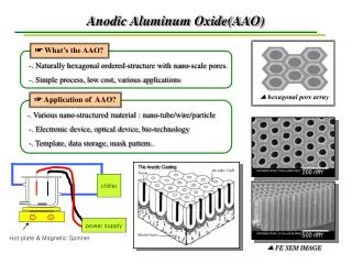
Motivation: General What is Anodic Porous Alumina? • Aluminum oxide grown on an Al substrate in an electrolytic cell. The resulting structure consists of an array of tunable nanometer-sized pores surrounded by an alumina backbone. Purpose: • To understand the mechanisms involved in the growth and ordering of anodic porous alumina. Motivation: • Interest in using anodic porous alumina as a nano- template to fabricate nanometer-sized structures (e.g. nanofabrication of quantum dots). Why do we want to fabricate nanostructures? • 1. Fundamental physical interest in the nanometer size regime. Properties of nano-sized structures are different from their bulk and molecular counterparts. • 2. Technological applications as electronic and optical devices.
Motivation: Applications Commercially available Anopore filter. http://www.2spi.com/catalog/spec_prep/filter2.html 1. Physics: • Explore optical, electrical, and magnetic quantum confinement. 2. Engineering: • Microfiltration. • Optical waveguides and photonic crystals for optical circuits. • Template for carbon nanotube growth for electronic, mechanical applications. • Ordered arrays of quantum dots for lasers, photodetectors. • ULSI memory devices and ICs. Porous Alumina used as optical waveguide. H. Masuda, et. al., Jpn. J. Appl. Phys.38, L1403 (1999). Ordered arrays of carbon nanotubes fabricated using a porous alumina template. J. Li, et al., Appl. Phys. Lett. 75(3), 367 (1999).
Overview of Anodic Oxide Films Fabrication • Anodizealuminum in electrolyte (e.g. Oxalic Acid) Two main types of anodic oxide films can be grown depending on the nature of the electrolyte: • 1. Barrier-Type Films: • Grown Oxide Insoluble in Electrolyte • Nearly Neutral Electrolytes (pH 5-7) • 2. Porous-Type Films: • Grown Oxide Slightly Soluble in Electrolyte • Aqueous Sulfuric, Oxalic, and Phosphoric Acid Electrolytes
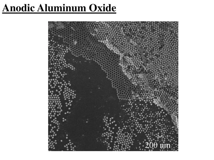
Porous Alumina Apparatus • Anodize aluminum in electrolyte (e.g. Oxalic Acid). • Oxide grows at the metal/oxide and oxide/electrolyte interfaces, pores initiate at random positions by field-assisted dissolution at the oxide/electrolyte interface. • Ordering requires appropriate potentials and long anodization times. • Ordering results from repulsion between neighboring pores due to mechanical stress at the metal/oxide interface. Resulting Structure H. Masuda and K. Fukuda, Science268, 1466 (1995).
Overview of Film Anodization • Oxide growth proceeds via ionic conduction and reaction of Al cations and oxygen containing anions under the influence of an applied field. (e.g. 2Al+ + 3OH- Al2O3+3H++6e-) • Pores initiate at random positions through field-assisted dissolution of the oxide at the oxide/electrolyte interface. • Initially oxide growth dominates. (I) • Dissolution becomes competitive, barrier layer thins, and pores initiate. (II) • Approaches steady state where both mechanisms occur at roughly the same rate. (III and IV) V.P. Parkhutik, and V.I. Shershulsky, J. Phys. D:Appl. Phys.25, 1258 (1992).
Ordered Nano-Templates Ordered Oxalic Near-Ordered Sulfuric • Tunable diameters and spacings from 20 nm to 500 nm. • Polycrystalline structure: ordered micron-sized domains, defects at grain boundaries. • Low temperature growth produces unordered 4-10 nm arrays.
Ordered Growth of Porous Alumina • Ordered pore arrays obtained in three different electrolytes for long anodization times and appropriate voltages (specific for each electrolyte). • Polycrystalline structure with perfectly ordered domains a few microns in size. Defects occur at grain boundaries.
Thermally Evaporated Nano-Dots: Gold • Porous alumina used as an evaporation mask to grow quantum dots. H. Masuda et al. , Jpn. J. Appl. Phys. 35, L126 (1996).
Overview: Mask Processing 1. Anodize sample for a long time to achieve ordered pores. 1. 2. Chemically remove the alumina in a mixture of phosphoric and chromic acid. 2. AFM of Unopened Barrier Layer (1 mm x 1 mm) 3. Anodize sample for a short time. 3. 4. Coat top surface of alumina with a polymer (collodion) to protect it from further processing. 4. 5. 5. Remove Al Substrate in a saturated HgCl2 solution. 6. 6. Remove the barrier layer in 5 wt.% Phosphoric Acid. 7. 7. Remove collodion and place alumina on desired substrate. H. Masuda et al. , Jpn. J. Appl. Phys. 35, L126 (1996).
Procedure: Anodization • Apply black wax around the area that you want to anodize. • Electropolish Aluminum surface to make it smooth. • Anodize the sample that should be ordered for 15 hours in oxalic acid. • Anodize the sample that should be disordered for 1 hour in oxalic acid.
Procedure: Anodization (cont.) • Chemically remove the alumina in a mixture of phosphoric and chromic acid. • Anodize both samples for one hour in oxalic acid. • Coat top surface of alumina with a polymer (collodion) to protect it from further processing.
Procedure: Anodization (cont.) • Remove Al substrate in a saturated HgCl2 solution. • Use a piece of silicon to pick up oxide and polymer and move to 5 wt. % phosphoric acid. This removes barrier layer. • Remove collodion and place alumina on desired substrate- silicon for SEM characterization and quartz for UV-Vis characterization.
Procedure: Thermal Evaporation Remove AAO with double stick tape. • Thermally Evaporate Gold onto all Samples • Must be done one sample at a time, because alignment is critical. • Gold layer should be ~50nm thick.
Results: SEM Characterization- silicon substrate Ordered AAO (100k magnification) Unordered AAO (100k magnification) Unordered Au dots (100k magnification) Ordered Au dots (100k magnification)
Results: UV-Vis Characterization- quartz substrate Ordered Array Disordered Array • Place drop of magic oil on microscope slide to get rid of Newton’s rings • Place sample in spectrophotometer. Scan from 300 to 1200nm.