Download
1 / 40
410 likes | 646 Views
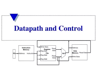
Datapath - performs data transfer and processing operations Control Unit - Determines the enabling and sequencing of the operations The control unit receives: External control inputs Status signals. The control unit sends: Control signals Control outputs.

E N D
Datapath - performs data transfer and processing operations Control Unit - Determines the enabling and sequencing of the operations The control unit receives: External control inputs Status signals The control unit sends: Control signals Control outputs Describe properties ofthe state of the datapath Control signals Status signals Control Control Datapath inputs unit Data outputs Control Data outputs inputs Datapath versus Control unit Henry Hexmoor
Two distinct classes: Programmable Non-programmable. A programmable control unit has: A program counter (PC) or other sequencing register with contents that points to the next instruction to be executed An external ROM or RAM array for storing instructions and control information Decision logic for determining the sequence of operations and logic to interpret the instructions A non-programmable control units does not fetch instructions from a memory and is not responsible for sequencing instructions This type of control unit is our focus in this chapter Control Unit Types Henry Hexmoor
The function of a state machine (or sequential circuit) can be represented by a state table or a state diagram. A flowchart is a way of showing actions and control flow in an algorithm. An Algorithmic State Machine (ASM) is simply a flowchart-like way to specify state diagrams for sequential logic and, optionally, actions performed in a datapath. While flowcharts typically do not specify “time”, an ASM explicitly specifies a sequence of actions and their timing relationships. Algorithmic State Machines Henry Hexmoor
State Box (a rectangle) Scalar Decision Box (a diamond) Vector Decision Box (a hexagon) Conditional Output Box (oval). The State Box is a rectangle, marked with the symbolic state name, containing register transfers and output signals activated when the control unit is in the state. The Scalar Decision Box is a diamond that describes the effects of a specific input condition on the control. It has one input path and two exit paths, one for TRUE (1) and one for FALSE (0). The Vector Decision Box is a hexagon that describes the effects of a specific n-bit (n > 2) vector of input conditions on the control. It has one input path and up to 2n exit paths, each corresponding to a binary vector value. The Conditional Output Box is an oval with entry from a decision block and outputs activated for the decision conditions being satisfied. ASM Primitives Henry Hexmoor
A rectangle with: The symbolic name for the state marked outside the upper left top Containing register transfer operations and outputs activated within or while leaving the state An optional state code, if assigned, outside the upper right top State Box (Optional state code) (Symbolic Name) IDLE 0000 (Register transfers or outputs) R ← 0 RUN Henry Hexmoor
A diamond with: One input path (entry point). One input condition, placed in the center of the box, that is tested. A TRUE exit path taken if the condition is true (logic 1). A FALSE exit path taken if the condition is false (logic 0). Scalar Decision Box (True Condition) (False Condition) (Input) 0 1 START Henry Hexmoor
A hexagon with: One Input Path (entry point). A vector of inputconditions, placed in thecenter of the box, that istested. Up to 2n output paths. The path taken has a binary vector value that matches the vector input condition (Binary Vector Values) (Binary Vector Values) (Vector of InputConditions) 00 10 01 Z, Q0 Vector Decision Box Henry Hexmoor
An oval with: One input path from a decision box or decision boxes. One output path Register transfers or outputs that occur only if the conditional path to the box is taken. Transfers and outputs in a state box are Moore type - dependent only on state Transfers and outputs in a conditional output box are Mealy type - dependent on both state and inputs Conditional Output Box From Decision Box(es) (Register transfers or outputs) R← 0 RUN Henry Hexmoor
By connecting boxes together, we begin to see the power of expression. IDLE R← 0 AVAIL 0 1 START PC ← 0 INIT Connecting Boxes Together Henry Hexmoor
One state box alongwith all decision andconditional outputboxes connectedto it is called an ASMBlock. The ASM Blockincludes all items on thepath from the currentstate to the same or otherstates. Entry IDLE ASM BLOCK AVAIL START R← R + 1 R ← 0 Exit 0 1 Q0 Exit Exit MUL1 MUL0 ASM Blocks Henry Hexmoor
Outputs appear while in the state Register transfers occur at the clock while exiting the state - New value occur in the next state! Clock cycle 1 Clock cycle 2 Clock cycle 3 Clock START Q 1 Q 0 MUL 1 IDLE State AVAIL 0034 0000 A ASM Timing Henry Hexmoor
Example: (101 x 011) Base 2 Note that the partial productsummation for n digits, base 2 numbers requires adding up to n digits (with carries) in a column. Note also nx m digit multiplygenerates up to an m + n digitresult (same as decimal). Multiplier Example • Partial products are: 101 x 0, 101 x 1, and 101 x 1 Henry Hexmoor
Reorganizing example to follow hardware algorithm: Example (1 0 1) x (0 1 1) Again || - concatenate Clear C || A Multipler0 = 1 => Add Addition Shift Right (Zero-fill C) Multipler1 = 1 => Add Addition Shift Right Multipler2 = 0 => No Add, Shift Right Henry Hexmoor
Multiplier Example: Block Diagram IN n 1 2 n Multiplicand Counter P Register B n log n 2 Zero detect G (Go) Parallel adder C out Z n n Multiplier Q Control o unit 0 C Shift register A Shift register Q 4 n Product Control signals OUT Henry Hexmoor
The multiplicand (top operand) is loaded into register B. The multiplier (bottom operand) is loaded into register Q. Register C|| Q is initialized to 0 when G becomes 1. The partial products are formed in register C||A||Q. Each multiplier bit, beginning with the LSB, is processed (if bit is 1, use adder to add B to partial product; if bit is 0, do nothing) C||A||Q is shifted right using the shift register Partial product bits fill vacant locations in Q as multiplier is shifted out If overflow during addition, the outgoing carry is recovered from C during the right shift Steps 5 and 6 are repeated until Counter P = 0 as detected by Zero detect. Counter P is initialized in step 4 to n – 1, n = number of bits in multiplier Multiplexer Example: Operation Henry Hexmoor
Multiplier Example: ASM ChartFigure 8-7 IDLE MUL0 0 1 G 0 1 Q 0 C ← 0, A ← 0 P← n – 1 A ← A + B, C ← C out MUL1 C← 0, C || A || Q← sr C || A || Q, 1 P← P – 0 1 Z Henry Hexmoor
Three states are employed using a combined Mealy - Moore output model: IDLE - state in which: the outputs of the prior multiply is held until Q is loaded with the new multiplicand input G is used as the condition for starting the multiplication, and C, A, and P are initialized MUL0 - state in which conditional addition is performed based on the value of Q0. MUL1 - state in which: right shift is performed to capture the partial product and position the next bit of the multiplier in Q0 the terminal count of 0 for down counter P is used to sense completion or continuation of the multiply. Multiplier Example: ASM Chart (continued) Henry Hexmoor
Multiplier Example: Control Signal Table Control Signals for Binary Multiplier Bloc k Dia g ram Contr o l Contr o l Mod u l e Mi cr oo pe ra ti on Si gn al N a me Exp r e ssi on ← IDLE · Register A : A 0 I nitia liz e G A ← A + B Load MUL0· Q ← C || A || Q sr C || A || Q Shift_dec M UL1 Register B : B ← IN Load_B LO ADB F lip-F lop C : C← 0 C lea r _C IDLE· G + MUL1 C ← C Load — ou t Register Q : Q ← IN Load_Q LO ADQ ← C || A || Q sr C || A || Q Shift_dec — – Cou n ter P : P ← n 1 I nitia liz e — ← – P P 1 Shift_dec — Henry Hexmoor
Signals are defined on a register basis LOADQ and LOADB are external signals controlled from the system using the multiplier and will not be considered a part of this design Note that many of the control signals are “reused” for different registers. These control signals are the “outputs” of the control unit With the outputs represented by the table, they can be removed from the ASM giving an ASM that represents only the sequencing (next state) behavior Multiplier Example: Control Table (continued) Henry Hexmoor
Multiplier Example - Sequencing Part of ASM IDLE 00 1 0 G MUL0 01 MUL1 10 0 1 Z Henry Hexmoor
Control Design Methods The procedure from Chapter 6 Procedure specializations that use a single signal to represent each state Sequence Register and Decoder Sequence register with encoded states, e.g., 00, 01, 10, 11. Decoder outputs produce “state” signals, e.g., 0001, 0010, 0100, 1000. One Flip-flop per State Flip-flop outputs as “state” signals, e. g., 0001, 0010, 0100, 1000. Hardwired Control Henry Hexmoor
Initially, use sequential circuit design techniques fromChapter 4. First, define: States: IDLE, MUL0, MUL1 Input Signals: G, Z, Q0 (Q0 affects outputs, not next state) Output Signals: Initialize, LOAD, Shift_Dec, Clear_C State Transition Diagram (Use Sequencing ASM on Slide 22) Output Function: Use Table on Slide 20 Second, find State Assignments (two bits required) We will use two state bits to encodethe three state IDLE, MUL0, and MUL1. Multiplier Example: Sequencer and Decoder Design Henry Hexmoor
Assuming that state variables M1 and M0 are decoded into states, the next state part of the state table is: Multiplier Example: Sequencer and Decoder Design (continued) Henry Hexmoor
Finding the equations for M1 and M0 is easier due to the decoded states: M1 = MUL0 M0 = IDLE · G + MUL1 · Z Note that since there are five variables, a K-map is harder to use, so we have directly written reduced equations. The output equations using the decoded states: Initialize = IDLE · G Load = MUL0 · Q0 Clear_C = IDLE · G + MUL1 Shift_dec = MUL1 Multiplier Example: Sequencer and Decoder Design (continued) Henry Hexmoor
Doing multiple level optimization, extract IDLE · G: START = IDLE · G M1 = MUL0 M0 = START + MUL1 · Z Initialize = START Load = MUL0 · Q0 Clear_C = START + MUL1 Shift_dec = MUL1 The resulting circuit using flip-flops, a decoder, and the above equations is given on the next slide. Multiplier Example: Sequencer and Decoder Design (continued) Henry Hexmoor
Multiplier Example: Sequencer and Decoder Design (continued) START Initialize G M 0 D Clear_C Z C DECODER IDLE A0 0 MUL0 1 MUL1 Shift_dec 2 A1 3 M 1 D C Load Q 0 Henry Hexmoor
This method uses one flip-flop per state and a simple set of transformation rules to implement the circuit. The design starts with the ASM chart, and replaces State Boxes with flip-flops, Scalar Decision Boxes with a demultiplexer with 2 outputs, Vector Decision Boxes with a (partial) demultiplexer Junctions with an OR gate, and Conditional Outputs with AND gates. Each is discussed detail below. Figure 8-11 is the end result. One Flip-Flop per State8-4 Henry Hexmoor
Each state box transforms to a D Flip-Flop Entry point is connected to the input. Exit point is connected to the Q output. State Box Transformation Rules Henry Hexmoor
Each Decision box transforms to a Demultiplexer Entry points are "Enable" inputs. The Condition is the "Select" input. Decoded Outputs are the Exit points. Scalar Decision Box Transformation Rules Henry Hexmoor
Each Decision box transforms to a Demultiplexer Entry point is Enable inputs. The Conditions are the Select inputs. Demultiplexer Outputs are the Exit points. (Binary Vector Values) (Binary Vector Values) (Vector of InputConditions) 00 10 01 X1, X0 Entry DEMUX Exit 0 D0 EN Exit 1 X1 D1 A1 Exit2 X0 A0 D2 Exit 3 D3 Vector Decision Box Transformation Rules Henry Hexmoor
Where two or more entry points join, connect the entry variables to an OR gate The Exit is the output of the OR gate Junction Transformation RulesFigure 8-11d Henry Hexmoor
Entry point is Enable input. The Condition is the "Select" input. Demultiplexer Outputs are the Exit points. The Control OUTPUT is the same signal as the exit value. Conditional Output Box RulesFigure 8-11e Henry Hexmoor
2 DEMUX D EN 0 D A 1 0 Multiplier Example: Flip-flop per State Design Logic Diagram 4 5 START Initialize IDLE 1 D 4 5 C Clear _C 2 MUL0 Q 1 0 DEMUX Load D D EN 0 G A D C 0 1 MUL1 1 5 D Shift_dec Clock C Z Henry Hexmoor
In processing each bit of the multiplier, the circuit visits states MUL0 and MUL1 in sequence. By redesigning the multiplier, is it possible to visit only a single state per bit processed? Speeding Up the Multiplier Henry Hexmoor
Examining the operations in MUL0 and MUL1: In MUL0, a conditional add of B is performed, and In MUL1, a right shift of C || A || Q in a shift register, the decrementing of P, and a test for P = 0 (on the old value of P) are all performed in MUL1 Any solution that uses one state must combine all of the operations listed into one state The operations involving P are already done in a single state, so are not a problem. The right shift, however, depends on the result of the conditional addition. So these two operations must be combined! Speeding Up Multiply (continued) Henry Hexmoor
By replacing the shiftregister with acombinational shifterand combining the adder and shifter,the states can be merged. The C-bit is no longer needed. In this case, Z and Q0have been made intoa vector. This is notessential to the solution. The ASM chart => IDLE 0 1 G A 0 P n – 1 MUL P P – 1 A || Q sr C || (A + 0) || Q A || Q sr C || (A + 0) || Q out out 00 10 Z || Q 01 11 0 A || Q sr C || (A + B) || Q A || Q sr C || (A+ B) || Q out out Speeding Up Multiply (continued) Henry Hexmoor
Microprogrammed Control — a control unit with binary control values stored as words in memory. Microinstructions — words in the control memory. Microprogram — a sequence of microinstructions. Control Memory — RAM or ROM memory holding the microinstructions. Writeable Control Memory — RAM Memory into which microinstructions may be written Microprogrammed Control Henry Hexmoor
Microprogrammed Control (continued) Henry Hexmoor
1. An ASM chart is given in Figure 8-19. Find the state table for the corresponding sequential circuit. (Q 8-3) 2. Manually simulate the process of multiplying the two unsigned binary numbers 1010 (multiplicand) and 1011 (multiplier). List the contents of registers A, Q, P, C and the control state, using the system in Figure 8-6 with n equal to 4 and with the hardwired control in Figure 8-12. (Q 8-12) HW 8 Henry Hexmoor