Download
1 / 37
370 likes | 462 Views
Project: IEEE P802.15 Working Group for Wireless Personal Area Networks (WPANs) Submission Title: High Power Miniature CVD Diamond-Based Submillimeter /Terahertz Signal Sources Date Submitted: 31 October, 2008 Source: Gerald T. Mearini Company: Teraphysics Corporation

E N D
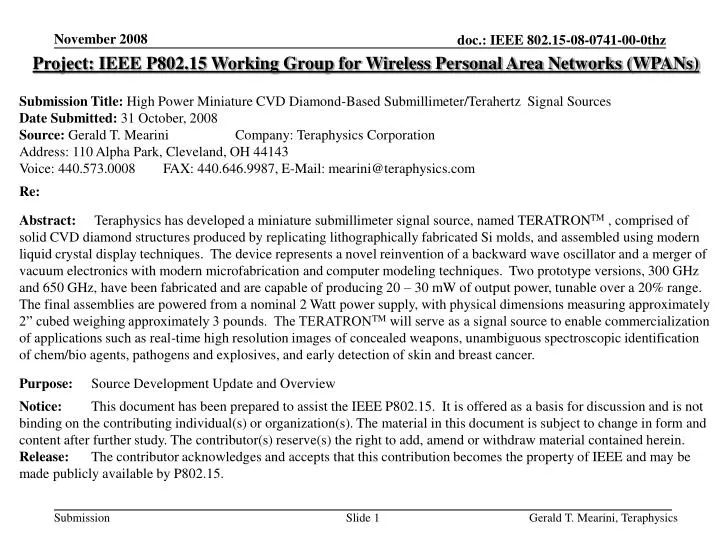
Project: IEEE P802.15 Working Group for Wireless Personal Area Networks (WPANs) Submission Title: High Power Miniature CVD Diamond-Based Submillimeter/Terahertz Signal Sources Date Submitted: 31 October, 2008 Source: Gerald T. Mearini Company: Teraphysics Corporation Address: 110 Alpha Park, Cleveland, OH 44143 Voice: 440.573.0008 FAX: 440.646.9987, E-Mail: mearini@teraphysics.com Re: Abstract:Teraphysics has developed a miniature submillimeter signal source, named TERATRONTM , comprised of solid CVD diamond structures produced by replicating lithographically fabricated Si molds, and assembled using modern liquid crystal display techniques. The device represents a novel reinvention of a backward wave oscillator and a merger of vacuum electronics with modern microfabrication and computer modeling techniques. Two prototype versions, 300 GHz and 650 GHz, have been fabricated and are capable of producing 20 – 30 mW of output power, tunable over a 20% range. The final assemblies are powered from a nominal 2 Watt power supply, with physical dimensions measuring approximately 2” cubed weighing approximately 3 pounds. The TERATRONTM will serve as a signal source to enable commercialization of applications such as real-time high resolution images of concealed weapons, unambiguous spectroscopic identification of chem/bio agents, pathogens and explosives, and early detection of skin and breast cancer. Purpose: Source Development Update and Overview Notice: This document has been prepared to assist the IEEE P802.15. It is offered as a basis for discussion and is not binding on the contributing individual(s) or organization(s). The material in this document is subject to change in form and content after further study. The contributor(s) reserve(s) the right to add, amend or withdraw material contained herein. Release: The contributor acknowledges and accepts that this contribution becomes the property of IEEE and may be made publicly available by P802.15.
Acknowledgements Funding NASA JPL Defense Advanced Research Projects Agency Army Research Office Air Force Office of Scientific Research Collaborators Teraphysics (C. Kory) RTI International (D. Malta, M. Lueck, K. Gilchrist) Hana Microdisplays (S. Worthington) Applied Diamond Lab (J. Tabeling) SRI International (C. Spindt, C. Holland) Naval Research Laboratory (J. Butler) TERAPHYSICS
Gold Diamond Biplanar Interdigital BWO (Patented 2007) • First proposed to NASA JPL in 2002 • Convergence of vacuum electronics, computer modeling and microfabrication • Interdigital structure formed on two planes • Diamond structure selectively metallized • Electric waves travel in the space between the planes • Electron beam passes between the planes and gives up energy to the electric waves
Thermal-Mechanical Advantages of Diamond • Highest known thermal conductivity • Relatively low permittivity • High strength • Artificial diamond can be grown in place using chemical vapor deposition (CVD) • CVD diamond forms intimate thermal bond with substrate • Unique application by Teraphysics
Fabrication Scheme Micro fabrication performed at RTI
100 mm Wafer Layout 300 GHz 6 V2 and 6 V2A 11 650 GHz V3 11 650 GHz V2 10 650 GHz VI Designed for wafer scale production
Patented Fabrication Process • Intricate structure designed on computer • Computer model transferred to silicon foundry • Negative of structure fabricated in silicon • Diamond grown into silicon molds • Silicon dissolved in acid leaving diamond replica of computer model • Direct transfer from computer file to diamond structure Diamond slow wave circuit Dimensions: 71.5 µm long, 86.5 µm high, 15.6 µm wide, 23.4 pitch
Two Views of Selective Metallization SEM Optical Microscope
Laser Dicing of BWO Bodies Accurate repeatable process 100 mm quarter wafer after dicing Adaptable to wafer scale production A Bucket of BWOs 100% yield on Lot 5, completed Oct. 22
BWO Layout Anode 1 Anode 2 Slow Wave Circuit Diamond Wall Electron Beam Path Antenna Field Emitter on Mesa Electron gun, slow wave circuit and antenna fabricated as an integrated diamond structure.
Field Emitter Layout SRI International Base Mesa is etched after field emitter is formed, greatly reducing yield.
Alignment Accuracy Hana Microdisplays
Assembly Steps Leaded 650 GHz V2B 650 GHz V1B BWO in alumina cradle
Remedial Action: OmniProbe Cathode mount • Silicon chips 220x800 micron diced at SRI • Tungsten needle inserted into silicon die • Micropositioner aligns die with mount • Die inserted into mount • Tungsten needle removed • Applicable to future manufacturability Die in BWO body
Remedial Action: Thermionic Gun Design for Planar BWO Diamond “forks” to facilitate alignment Field emission gun removed with laser dicing Computer simulations for optimized design 500 Alignment of gun and circuit challenging Miniature thermionic gun layout Cathode
Planar BWO Project Technology Innovations • Computer-aided design of gun, circuit, and antenna • Transfer CAD file to Si mask to diamond structure • DRIE of SOI wafers to create Si mold • CVD growth of diamond structures in Si mold • Grow flat, transparent diamond of correct thickness • Self masking of diamond structure for selective metallization • Vertical metallization of gun electrodes • Fabrication of field emitter arrays • Laser dicing of individual BWO halves • Prototype BWOs assembled using LCD technology • Application of micromanipulator for cathode insertion • Design of miniature thermionic electron gun • Demonstrate BWO operation
Predicted Characteristics of Planar BWO • Continuous wave operation • Frequency is continuously voltage tunable • Voltage 6 kV, current 2.0 mA • BWO power 26 mW at 6 kV, 125 mW at 12 kV • Efficiency 1.8 % (10x improvement) • Mass of magnetic circuit 1.6 kg • Designed for wafer scale production
Next Generation: ConventionalHelical Slow Wave Circuit • Most commonly used slow wave circuit. • Advantages: wide bandwidth, high efficiency, moderate power, broad manufacturing base, vast expository literature. • Fabricated by winding wire or tape around a mandrel. • Supported in center of barrel by dielectric rods. • Seldom fabricated for applications above 50 GHz because of high beam interceptionand mechanical and thermal stress
Lithographically Fabricated Helical Slow Wave Circuits • Helix fabricated lithographically • Diamond dielectric support structure • Electron gun and barrel fabricated as a unit • Wafer-level economies of scale • 160 BWOs from four 100 mm wafers • Output power radiated directly from circuit • Electron beam encircles helix • Applicable to W-band and sub mm devices Patent Application Submitted Feb. 2008
Doubly Convergent Electron Gun • Side cut through view of electron gun designed at 95 GHz • Beam trajectories through gun showing double convergence Doubly Convergent Gun: First the beamlets are focused to increase current density. At the same time the beamlets must be drawn into trajectories of reduced radius, parallel to the axis. Provisional Patent Application • End view of particles through circuit showing 100% beam transmission
Novel Helical Circuit Design and Fabrication • Golden helix supported by a diamond sheet in a diamond box that has been selectively metallized on the inside • The electron beam passes through space above and below helix • Fabrication process flow
Isotropic Etch and Selective Metallization of Circular Trenches Depth and shape of trench controlled by etch conditions. Mold for half helix Half helix
Au/Au Die Bonding Half helix with bonding bumps Helix section after bonding Complete helix has 306 bonds: 100% yield
Accidents Will Happen The bonds did not break!
Helix Perspective Diameter of human hair
Fabrication of Helix on Diamond Sheet Trench etched in diamond sheet Half helix on diamond sheet Simulation of RF currents in helix Helix on diamond sheet
Iterative Helical Design and Fabrication • Gold helix bonded to diamond sheet • Electroplated gold helix in silicon trench without diamond sheet • Three simulated helices having the same RF properties illustrating the capability to design the circuit around the resulting fabricated helices
Masks for Diamond Box Dark green areas are oxide and resist (final ridge height of 190 um), blue areas are resist only (final ridge height of 100 um) Wafer Die Matching top and bottom device pairs
SEM images from wafer 2 Low mag SEM image of wafer 2 showing the waveguide coupler area SEM image of the waveguide and slow wave circuit areas
Helical BWO Assembly A golden coil supported by a diamond sheet and suspended within a diamond box Four 100 mm wafers will produce 160 BWOs in a single operation
Summary These concepts extend the applicable frequency range of the helical slow wave circuit by more than an order of magnitude. Computer modeling of idealized structures is starting point for development. Feasibility of essential fabrication procedures is demonstrated. Computer simulations and fabrication experiments are proceeding iteratively for a 95 GHz TWT (AFOSR) and a 650 GHz BWO (ARO). 650 GHz is not the upper limit for the lithographically fabricated helix. Proposal to DARPA pending for TWTs at 670, 830 and 1030 GHz. Family of devices with higher power and frequency enables a wide range of applications
Properties of THz Radiation Relevant to Major Applications Harmless nonionizing radiation All warm bodies naturally emit THz radiation THz radiation will pass through clothing (and bandages) Complex molecules can be identified by their resonant signatures in THz band Speed and attenuation of light in water (and blood) changes dramatically in THz band Distinctively different propagation in different types of human tissue Selective heating below surface of the skin possible THz radiation strongly attenuated in atmosphere High frequency implies broad bandwidth and very high wireless data transmission rates
Potential Applications Medical Wound Imaging: THz radiation will pass through bandages, allowing medical personnel to inspect wounds without disturbing healing process. In Situ Cancer Imaging: During surgery THz radiation reflects from a tumor differently because it contains an abnormal concentration of blood. Skin Cancer Imaging: THz radiation can provide images of cancers growing on or near surface of skin. Mammography: THz radiation may be able to detect and identify abnormalities in breast tissue without subjecting patient to invasive procedures. Prostate Cancer Detection: THz radiation may be able to detect and identify abnormalities in prostate tissue with greater resolution throughout entire volume of organ. Pharmaceuticals: THz radiation can be used to identify counterfeit drugs, point of sale confirmation of drug identity, verify thickness and density of coatings on time release capsules, and provide quality assurance. Dentistry: THz radiation may be able to provide images of dental carries without subjecting patient or the medial practitioner to ionizing radiation. Cosmetics: THz radiation has been proposed as means to heat subcutaneous collagen to smooth wrinkled skin. • Homeland Security • Devices will enable sensing at safe distance of weapons and other contraband hidden under clothing of persons approaching military checkpoints or entrances to critical facilities, airport terminals, etc. • These systems may make it possible to accurately identify in real time the distinct signatures of complex molecular substances present in the environment such as dispersed aerosols and toxic gases. • Communications • The wide bandwidth of these TWTs will enable secure very high data rate wireless interconnections between computers or in enclosed spaces such as aircraft cockpits. • Space Science • NASA determines the composition of dark space in the universe by detecting the characteristic resonances of molecules in deep space using a highly sensitive spectrometer. THz radiation has been used to inspect the tiles on the space shuttle. • Electronics • Detection of defects in materials and microprocessor circuits using time delayed reflectometry.