Download
1 / 3
30 likes | 136 Views
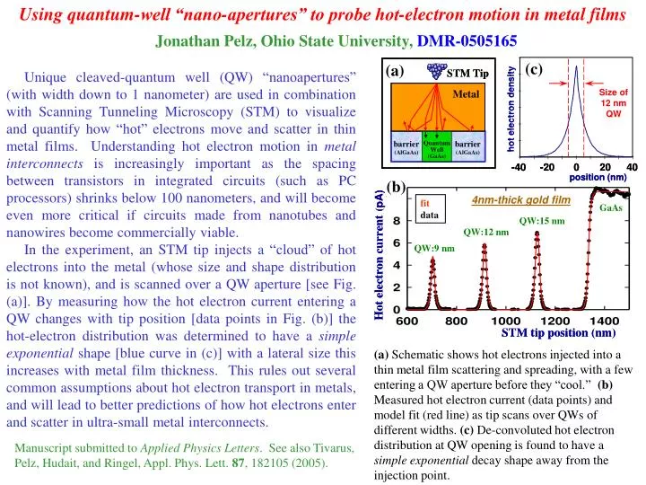
Using quantum-well “nano-apertures” to probe hot-electron motion in metal films Jonathan Pelz, Ohio State University, DMR-0505165. (c). (a). Size of 12 nm QW. (b).

E N D
Using quantum-well “nano-apertures” to probe hot-electron motion in metal films Jonathan Pelz, Ohio State University,DMR-0505165 (c) (a) Size of 12 nm QW (b) (a) Schematic shows hot electrons injected into a thin metal film scattering and spreading, with a few entering a QW aperture before they “cool.” (b) Measured hot electron current (data points) and model fit (red line) as tip scans over QWs of different widths. (c) De-convoluted hot electron distribution at QW opening is found to have a simple exponential decay shape away from the injection point. Unique cleaved-quantum well (QW) “nanoapertures” (with width down to 1 nanometer) are used in combination with Scanning Tunneling Microscopy (STM) to visualize and quantify how “hot” electrons move and scatter in thin metal films. Understanding hot electron motion in metalinterconnects is increasingly important as the spacing between transistors in integrated circuits (such as PC processors) shrinks below 100 nanometers, and will become even more critical if circuits made from nanotubes and nanowires become commercially viable. In the experiment, an STM tip injects a “cloud” of hot electrons into the metal (whose size and shape distribution is not known), and is scanned over a QW aperture [see Fig. (a)]. By measuring how the hot electron current entering a QW changes with tip position [data points in Fig. (b)] the hot-electron distribution was determined to have a simple exponential shape [blue curve in (c)] with a lateral size this increases with metal film thickness. This rules out several common assumptions about hot electron transport in metals, and will lead to better predictions of how hot electrons enter and scatter in ultra-small metal interconnects. Manuscript submitted to Applied Physics Letters. See also Tivarus, Pelz, Hudait, and Ringel, Appl. Phys. Lett. 87, 182105 (2005).
Imaging electron transport at nanometer-sized “pinholes” in molecular monolayers (a) (b) (c) (a) Schematic cross section showing nm-sized, metal-filled pinholes through a dC-X molecular film. (b) Metal grain structure and (c) simultaneous BEEM image of sub-surface pinholes through molecular film. Blue dots show locations where local SBHs were measured, which were significantly increased by the surrounding dC-X film. Jonathan Pelz, Ohio State University,DMR-0505165 There is great world-wide effort to incorporate thin films of electronically-active organic molecular materials with semiconductor-based circuits, to combine synthetic chemistry’s power to design molecular functionality with the scalability of existing semiconductor fabrication technology. However, the uniformity and electronic properties of these new molecule/semiconductor and molecule/metal interfaces are not yet well understood or optimized. The PI’s group (in collaboration with the Weizmann Institute in Israel) used nm-resolution Ballistic Electron Emission Microscopy (BEEM) to image the spatial integrity and electronic behavior of metal/dC-X/GaAs stacks, where dC-X is a discontinuous monolayer of dicarboxylic acids with different functional end group. BEEM imaged the metal grains in the top metal film [Fig. (b)] simultaneously with the nm-sized pinholes in the buried molecular film [white spots in Fig. (c)]. It also showed that the molecular film surrounding individualpinholes significantly increased the local Schottky barrier height (SBH), which is the energy needed by electrons to enter the GaAs through the pinholes. Collaborations with other groups are currently underway to investigate how molecular type and film processing affect electron energy levels and magnetic behavior in different molecular films. H. Haick, et al., Phys. Stat. Sol. (A) 203, 3438 (2006).
Interdisciplinary Training, Collaborations, and Outreach Jonathan Pelz, Ohio State University,DMR-0505165 Ballistic Electron Emission Microscopy (BEEM) images measured over cleaved GaAs quantum wells with embedded InGaAs quantum dots. Demonstrating conservation of energy and momentum to 6th grade students. Interdisciplinary Training: With NSF support, two undergraduate REU students (Corey Campbel and Steven Stone) and three graduate students (Camelia Marginean, Cristian Tivarus, and Yulu Che) received highly interdisciplinary training using advanced techniques in technologically important topics in nanoscience. Collaboration with Undergraduate Institutions: Professor Pelz collaborates with Professor Susan Lehman and her students of the College of Wooster to study nanometer scale electronic behavior of “cleaved quantum dots” (top figure) resulting so far in a March Meeting presentation for Prof. Lehman and a manuscript in preparation. Outreach: The PI regularly presents physics demonstrations in elementary school classrooms (1st – 6th Grade), and has worked with elementary school teachers to help prepare for the Ohio State Proficiency Test. This year, the PI is also advising a local middle school teacher and student team for the “National Engineers’ Week Future City Competition” (see http://www.futurecity.org). This year’s essay topic is “Keep our Future City’s Infrastructure Healthy: Using Nanotechnology To Monitor City Structures and Systems.”