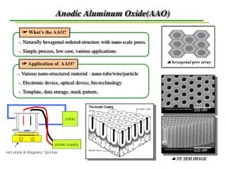
Download
1 / 10
100 likes | 601 Views
非晶態透明導電氧化物薄膜 Amorphous Transparent Conducting Oxide Films. 劉旭禎 臺師大 林口校區 數理學科. 劉旭禎 國立交通大學 電子物理系 博士 (2002.12) 現職與經歷 : 臺師大 林口校區 數理學科 (2008.2~ 迄今 ) 明志科技大學材料工程系 (2005.8~2008.1) 工研院電子所與材料所 (2003.7~2005.7) 交大電物系博士後研究 (2003.2~2003.6). Electron energy. Conduction band. band gap.

E N D
非晶態透明導電氧化物薄膜 Amorphous Transparent Conducting Oxide Films 劉旭禎 臺師大 林口校區 數理學科
劉旭禎 國立交通大學 電子物理系 博士 (2002.12) 現職與經歷: 臺師大 林口校區 數理學科 (2008.2~迄今) 明志科技大學材料工程系 (2005.8~2008.1) 工研院電子所與材料所 (2003.7~2005.7) 交大電物系博士後研究 (2003.2~2003.6)
Electron energy Conduction band band gap Valence band • 透明導電氧化物薄膜 • 可見光波長 400 ~ 700 nm (3.1 ~ 1.77 eV) • 半導體能隙 < 1.77 eV: 吸收可見光 黑色 • 半導體能隙 > 3.1 eV : 不吸收可見光 透明 • 寬能隙半導體: 能隙 ~ 3 eV GaN, ZnS, ZnO…
SnO2 ZnO In2O3 rutile wurtzite bixbyite Transparent Conducting Oxides SnO2:F (FTO) SnO2:Sb (ATO) ZnO:Al (AZO) ZnO:Ga (GZO) In2O3:Sn (ITO)
LCD Zn1-xAlxO solar cell • 透明導電氧化物薄膜的應用 • 平面顯示器(LCD, PDP) • 太陽電池(solar cell…) • 2. 低輻射玻璃(low-E glass) • 3. 雙抗鏡片(抗UV, 抗輻射)
非晶態透明導電氧化物薄膜 • InGaZnO4 (IGZO) • Flexible Transparent TFT • 特性: • 室溫製程 (紙張) • 透明且可撓 • 高遷移率 (~10 cm2/Vs) (a-Si~1 cm2/Vs ) Oxygen 2p orbital Metal ns orbital (n≧4) Si InGaZnO4 K. Nomura et al., Nature 432, 488 (2004).
最近的工作: • Mn-, Cr-doped IGZO films (PLD) • Mo-doped IGZO films (co-sputtering) Mn-doped IGZO films S. J. Liu et al., Appl. Phys. Lett. (2009)
未來研究: • 過渡金屬元素摻雜對非晶態透明導電氧化物薄膜物理特性之影響 (國科會三年計畫) • In-Ga-Zn-O:嘗試以其他元素取代In, 並製作TFT(交大) • 研究設備(一): • 試片製作與處理: • 1. 2-gun 濺鍍系統: 2” target, 4” wafer • 2. 脈衝雷射鍍膜系統: (交大, 新竹) • 2. 材料結構與特性分析: AFM, XRD, EDX, TEM… • (明志科大, 泰山)
研究設備(二): 3. 物理特性量測: a.電性量測: Keithley 2400: I & V source, I &V measurement Picotest M3500A: I, V, R measurement Keithley 2182A: nano-volt meter (將採購) b. 光學量測: UV/Vis/NIR 光譜儀: 透光率與反射率 (將採購) c. 磁性量測: SQUID:M-T & M-H (交大, 新竹)
畢業生出路: • 交大 光電所 博士班 1 位 • 交大 材料系 博士班 1 位 (明志科大碩士生) • 友達光電 3 位 • 服役 2 位 劉旭禎 林口校區 科學館三樓 sjliu@ntnu.edu.tw 02-77148400 Welcome to Linkou Campus