Download
1 / 35
410 likes | 730 Views
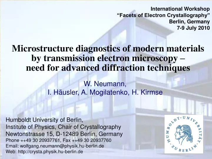
International Workshop “Facets of Electron Crystallography” Berlin, Germany 7-9 July 2010. Microstructure diagnostics of modern materials by transmission electron microscopy – need for advanced diffraction techniques. W. Neumann, I. Häusler, A. Mogilatenko, H. Kirmse.

E N D
International Workshop “Facets of Electron Crystallography” Berlin, Germany 7-9 July 2010 Microstructure diagnostics of modern materials by transmission electron microscopy – need for advanced diffraction techniques W. Neumann, I. Häusler, A. Mogilatenko, H. Kirmse Humboldt University of Berlin, Institute of Physics, Chair of Crystallography Newtonstrasse 15, D-12489 Berlin, Germany Phone ++49 30 20937761, Fax ++49 30 20937760 Email: wolfgang.neumann@physik.hu-berlin.de Web: http://crysta.physik.hu-berlin.de
Adlershof Campus – City of Science and Industry Humboldt University of Berlin Institute of Physics Chair of Crystallography Newtonstrasse 15 D-12489 Berlin Germany
Joint Laboratory for Electron Microscopy Adlershof (JEMA) • TEM/STEM JEOL 2200 FS • Field emission gun • U = 200 kV • Point resolution: 0.19 nm • STEM resolution: 0.14 nm • Energy resolution: 0.7 eV • Focused ion beam system FEI FIB Strata 201 • TEM specimen preparation • Cross sections • Target preparation • Surface morphology tailoring • Ion beam diameter: 20 nm
Tomography TEM/STEM IMAGING DIFFRACTION SPECTROSCOPY Phasecontrast (high-resolution imaging) Energy dispersive X-ray spectroscopy Amplitudecontrast (diffraction contrast) Selected area diffraction Electron energy loss spectroscopy Convergent beam diffraction Micro-/nano- diffraction Electron holography Z-contrast imaging X-ray mapping Energy-filtered TEM (EFTEM) Lorentz microscopy
Tomography TEM/STEM IMAGING DIFFRACTION SPECTROSCOPY Phasecontrast (high-resolution imaging) Energy dispersive X-ray spectroscopy Amplitudecontrast (diffraction contrast) Selected area diffraction Electron energy loss spectroscopy Convergent beam diffraction Micro-/nano- diffraction Electron holography Z-contrast imaging X-ray mapping Energy-filtered TEM (EFTEM) Lorentz microscopy Precession
Characterization of single crystalline LiAlO2 substrates for subsequent GaN epitaxy
(0001)GaN (1100)GaN LiAlO2(100) substrates for GaN based optoelectronics -6.3% in b-1.4% in c -0.1% in b-1.4% in c • Almost a lattice matched substrate for GaN epitaxy; • LiAlO2(100) allows the growth of both polar c-plane and non-polar m-plane GaN; • Fabrication of free standing GaN waffers, which can be used as substrates for subsequent homoepitaxy; • LiAlO2 self-separation from thick GaN layers
(001) cut Growth of -LiAlO2(100) single crystals by Czochralski technique FWHM < 40 arcsec inclusions Problem: Li2O evaporation from the surface of the growing crystal or melt during the single crystal growth B. Velickov et al., Journal of Cryst. Growth 310 (2008) 214 Institute of Crystal Growth - Berlin
inclusions LiAlO2 Inclusions in -LiAlO2 no common orientation relation to matrix idiomorphic shape EDXS: inclusions matrix
Phase analysis of inclusions in -LiAlO2 Problems: a large number of possible phases, i.e. LiAl5O8, Al2O3, -, -, -LiAlO2 modifications inclusions are not homogeneously distributed in the -LiAlO2 matrix, so that it is difficult to localize them during the specimen preparation Solutions: 1. electron diffraction analysis along a number of low index zone axes 2. possibly ELNES- analysis of oxygen K-edge Way: 1. prepare a large number of specimens (time consuming) and tilt, tilt, tilt 2. simulate fine structure of O-K edge for different phases and look if you can distinguish between them with energy resolution available at your TEM
Electron diffraction evidence for formation of LiAl5O8 Explanation: Li2O loss from the melt resulting in formation of unsolvable LiAl5O8 inclusions. - number of prepared specimens: 13 - invested time: 1 year B. Velickov et al., Journal of Cryst. Growth 310 (2008) 214
ELNES evidence for formation of LiAl5O8 LiAlO2 matrix LiAl5O8 inclusion electron energy filter with a proper energy resolution is necessary time consuming simulations are necessary W. Hetaba et al., Micron 41 (2010) 479
FePt, L10 (fct) FePt, A1 (fcc) a = 0.380 nm a = c a = 0.385 nm c = 0.371 nm Disorder-order transformation in FePt chemically ordered phase disordered phase T Chemically ordered L10 phase shows a high uniaxial magnetic anisotropy promising candidate for high-density magnetic recording media
Phase determination in single crystalline FePt nanocrystals HAADF STEM: J. Biskupek et al., Ultramicroscopy 110 (2010) 820 degree of chemical order
Phase determination in single crystalline FePt nanocrystals chemically ordered phase disordered phase FePt, L10 (fct) FePt, A1 (fcc) Structure factor: T Electron diffraction: in [100] zone axis • kinematically forbidden for a random phase. • allowed for a chemically ordered phase
Electron diffraction analysis of polycrystalline FePt layers on Si CHEMNITZ UNIVERSITY OF TECHNOLOGY Group of Surface and Interface Physics as-deposited FePt layers chemically disordered (fcc) FePt experimental patternwith FePt simulation FePt: a = 0.380 nm experimental patternwith Pt simulation Pt: a = 0.391 nm Result: no Pt!
HRTEM analysis of polycrystalline FePt layers 2 nm as-deposited FePt layers chemically disordered (fct) FePt 2 nm FFT IFFT 70.5° FePt fcc: angle beween (1-11) and (1-1-1) is 70.53° FePt fct: angle beween (1-11) and (1-1-1) is 72.54° 72.5°
glue FePt SiO2 spheres SiO2 Si 400 nm CHEMNITZ UNIVERSITY OF TECHNOLOGY Group of Surface and Interface Physics FePt crystallites on self-assembled SiO2 nanospheres FePt on the 100 nm SiO2 spheres + annealing annealing should initiate the formation of chemically ordered fct phase!
Pt Fe Si FePt crystallites on self-assembled SiO2 nanospheres EDXS mapping: HAADF STEM: 100 nm 55 at. % Pt, 45 at .% Fe ± 5 at.%
100 fct 111 fcc 200 fcc Phase determination in FePt nanocrystals on self-assembled SiO2 nanospheres Electron diffraction: Problem: low number of diffraction reflections Possible solution: precession electron diffraction
Material system: MnAs/GaAsMotivation Phase transformation of MnAs: 40°C 125°C 250°C Temperature b - MnAs orthorhombicparamagnetic a - MnAs hexagonalferromagnetic g - MnAs hexagonalparamagnetic
Material system: MnAs/GaAsMotivation Phase transformation of MnAs: 40°C 125°C 250°C Temperature b - MnAs orthorhombicparamagnetic a - MnAs hexagonalferromagnetic g - MnAs hexagonalparamagnetic Spintronic devices : • Exploitation of the intrinsic spin of the electron and its associated magnetic moment, in addition to its fundamental electronic charge Advantages over conventional electronic devices: • Faster and more efficient devices • Processing and handling of an higher information density • Low heat development
Growth of MnAs/GaAs Structure Growth technique Properties 1-dim: MnAs/GaAs Nanowires 2-dim: MnAs/GaAs Layers 3-dim: MnAs/GaAs crystallites MOCVD MBE MOCVD non magnetic a-MnAs (ferromagnetic) a-MnAs (ferromagnetic)
Cluster Growth of MnAs/GaAs Structure Growth technique Properties 1-dim: MnAs/GaAs nanowires 2-dim: MnAs/GaAs layers 3-dim: MnAs/GaAs crystallites MOCVD MBE MOCVD non magnetic a-MnAs (ferromagnetic) a-MnAs (ferromagnetic) Curie-Temperatur TC > 330 K
Material system: MnAs-crystallite / [001] GaAs plan view bright field TEM image cross section bright field TEM image MnAscrystallite MnAs crystallite GaAs matrix GaAs matrix
HRTEM GaAs (Mn,Ga)As
Material system: MnAs-crystallite / [001] GaAs FFT GaAs matrix (Ga,Mn)As crystallite
Material system: MnAs-crystallite / [001] GaAs FFT GaAs matrix PS || [1-101] Sim. (Ga,Mn)As crystallite
GaAs cubic MnAs orthorhombic MnAs hexagonal Material system: MnAs-crystallite / [001] GaAsPhase map virtual bright field phases 1 mm Nano beam diffraction Spot size: 2.4 nm 1 mm b-MnAs orthorhombic phase (paramagnetic)
Material system: MnAs-crystallite / [001] GaAsOrientation maps
[010] [001] [100] [110] [001] [110] Material system: MnAs-crystallite / [001] GaAsOrientation maps GaAs [010] [100] MnAs (orthorhombic) [001]
Scientific contributions of Anna Mogilatenko Holm Kirmse Ines Häusler