Download
1 / 8
80 likes | 86 Views
An Investigation on shielding enclosure for EMI<br>An Investigation on shielding enclosure for EMI<br>An Investigation on shielding enclosure for EMI

E N D
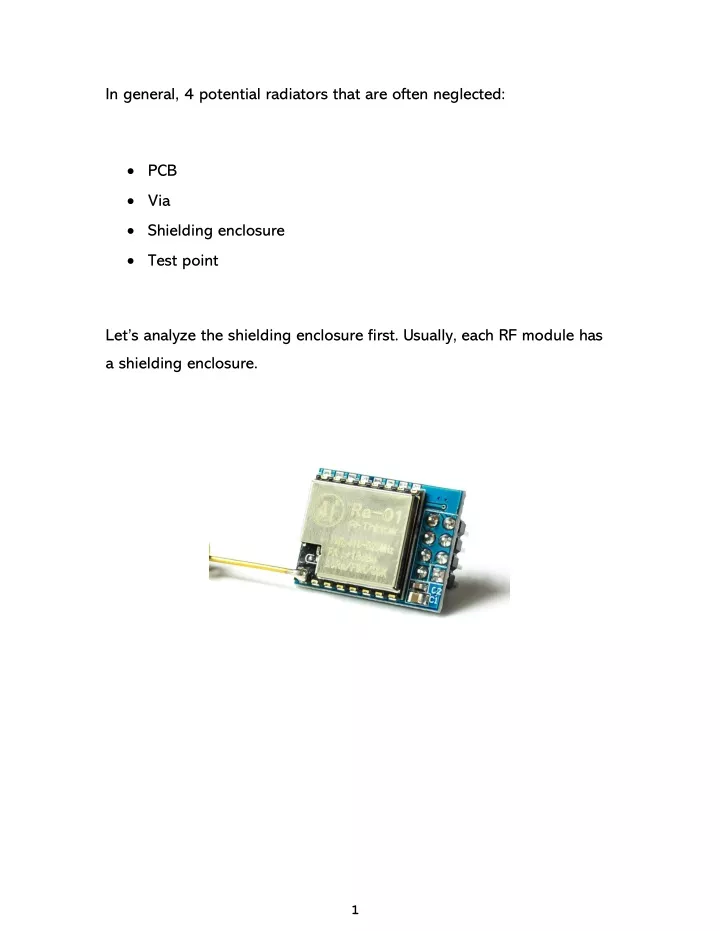
In general, 4 potential radiators that are often neglected: PCB Via Shielding enclosure Test point Let’s analyze the shielding enclosure first. Usually, each RF module has a shielding enclosure. 1
As shown above, a metal cavity resonator (red rectangular) is composed of a shielding enclosure, GND via, and the main GND plane. To put it another way, it would be a potential radiator [1]. Noise source would be chip itself, and it couples to the shielding enclosure. And, the noise on the shielding enclosure can be expressed as: Coupled Noise = Radiation + flow to main GND 2
In other words, one part of the noise would radiate outside; the other part would flow to the main GND plane. As mentioned earlier, the shielding enclosure would be a potential radiator thanks to the cavity resonator. Thus, according to the previous formula, the radiation is inevitable. What’s more, how much it radiates depends on the quality of grounding. We list the most extreme cases: Coupled Noise Coupled Noise Radiation Flow to main GND 100% 0% Poor Grounding Good Grounding 0% 100% To put it another way, you can suppress the radiation by enhancing the grounding. 3
Small Module Top Layer GND vias GND Plane Big Module Top Layer GND vias GND Plane Therefore, in terms of grounding, the grounding quality of a small module is worse than that of a big module. Since the area of shielding enclosure of a small module is smaller than that of a big one. That is, the number of GND via of a small module is lower than that of a big module. Every via has its internal resistance, and we assume it’s R. 4
The more the number of parallel resistors is, the lower the total resistance is. In this respect, small module MUST have worse grounding quality than that of a big module since a small module has fewer GND vias thanks to its smaller area of shielding enclosure. Consequently, the shielding enclosure of a small module would radiate outside more easily than how a big module does. In terms of rectangular cavity resonator, Different dimensions lead to different resonant frequencies. 5
Take 915 MHz, the Lora spectrum (North America), for example, the chances are that 915 MHz corresponds with those resonances of a small module but doesn’t correspond with that of a big one. As mentioned earlier, the grounding quality of a small module is worse. So, with that, the shielding enclosure of a small module may radiate outside thanks to the cavity resonator mechanism, thereby radiating to the antenna and interfering with the received signal. Look at another real case. There’s a de-sense issue in WIFI 5 GHz application. As shown below: The radiated interference reduced much with a cut in the SD card connector. 6
Let’s analyze this phenomenon by what we mentioned previously. In general, a de-sense issue is composed of 4 elements: noise source, radiator, path, and receptor. Basically, the de-sense would be mitigated as long as one of these elements is removed. A cut on the SD card connector means changing the dimension of the cavity resonator, thereby altering its resonant frequencies. The chances are that new resonant frequencies avoid WIFI 5 GHz band, and the issue is solved. 7
Reference Reference [1] EMC techniques in electronic design Part 4 – Shielding 8