Download
1 / 24
260 likes | 396 Views
AC97 PCM Audio. EECS150 Fall 2007– Lab Lecture #6 Udam Saini. Today. Checkpoint #1 Block Diagram Requirements AC97 Audio Administrative Info Reset & Timing Volume Controls Simulation Model. Checkpoint #1 (2). Checkpoint #1 (3). Requirements Record and Play digital audio

E N D
AC97 PCM Audio EECS150 Fall 2007– Lab Lecture #6 Udam Saini EECS150 Lab Lecture #6
Today • Checkpoint #1 • Block Diagram • Requirements • AC97 Audio • Administrative Info • Reset & Timing • Volume Controls • Simulation Model EECS150 Lab Lecture #6
Checkpoint #1 (2) EECS150 Lab Lecture #6
Checkpoint #1 (3) • Requirements • Record and Play digital audio • Use our audio fifo that we give you to store the audio bits. • Holds only 8 seconds on audio. • Implement Volume Controls • Use the dipswitches to control the volume/mute levels. EECS150 Lab Lecture #6
Checkpoint #1 (4) • Interfacing to external chips • Exact Requirements • Detailed timing and interface specifications • If you get it wrong, who knows what happens? • Datasheets • Detailed specification document • Includes EVERYTHING you need to know • Simulation • Often not possible • We’re going to help you out here… EECS150 Lab Lecture #6
Checkpoint #1 (5) • To Do List (Not RTL or STD) • Ensure AP_RESET_ is held long enough • We’ll help you out on this one • Continuously generate AP_SYNC • Wait for CodecReady • Initialize AC97 Control Registers • Send Volume Commands • Store PCM Data • Play PCM Data EECS150 Lab Lecture #6
AC97 Audio (1) EECS150 Lab Lecture #6
AC97 Audio (2) • Serial Bit Stream • You must generate a sync signal • Two Parts to AC97 • Command Data (Read/Write Registers) • PCM (Wave) audio data • The Chip • LM4549A Audio Codec • READ THE DATASHEET (Its short) EECS150 Lab Lecture #6
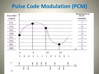
AC97 Audio (3) • Bit serial transmission • AP_SDATA_OUT is from FPGA to Codec • AP_SDATA_IN is from Codec to FPGA • Data transmitted in 256b frames • 13 slots per frame • Slot0 is 16b • Slots1-12 are 20b • Sync signal high (roughly) during Slot0 EECS150 Lab Lecture #6
AC97 Audio (4) EECS150 Lab Lecture #6
AC97 Audio (5) • Slot0 - Tag • Bit[15] - 1 is frame is valid • Bits[14:11] - 1 if corresponding slot is valid • Bits[10:2] - Not Used • Bits[1:0] - ID, set to 2’b00 • Slot1 - Register Address • Slot2 - Register Data (for writes) • Slots3&4 - PCM Audio Data EECS150 Lab Lecture #6
AC97 Audio (6) EECS150 Lab Lecture #6
AC97 Audio (7) • Command Registers • Control Volume/Mute • Control PCM Audio Rate • You’ll need to set this to FA0(4000) at reset EECS150 Lab Lecture #6
AC97 Audio (8) EECS150 Lab Lecture #6
Administrative Info (3) • Deadlines • Checkpoint 1 • Design Review – Due next week in lab • Checkoff – Due the following week in lab. • Your design should be detailed enough that you could give your design to another group and have them implement it from scratch. • GET YOUR CHECKPOINTS DONE EARLY • Don’t wait for the deadline, you will fall behind EECS150 Lab Lecture #6
Reset & Timing (2) • LocalResetGen • Generates resets for use with gated clocks • Key components: • Ability to hold reset high using a counter • Shift register to cross clock domains • Timeout in the event that the local clock dies • Multiple reset outputs • Outputs • LocalClockReset – Resets the clock generator • LocalRegReset – Resets all the registers EECS150 Lab Lecture #6
Reset & Timing (3) • AC97 Sync • First high SAMPLE marks start of frame • Not the first time you drive it high • What’s the difference? • Should be high for 16 cycles (Slot 0) • This is CRITICAL • Without proper sync the codec won’t work • This signal is how the codec finds the start of the AC97 frame EECS150 Lab Lecture #6
Volume Controls (2) • Features • Inputs • Speaker Volume/Mute • Mic Volume/Mute • Outputs • Contents of the corresponding AC97 register • We recommend modular design EECS150 Lab Lecture #6
Simulation Model (1) • We built you a model • LM4549ACodec.V • This is for simulation ONLY • It error checks the AC97 data • Limitations • This model is not perfect • It may in fact have bugs • Do not rely on only this model • On board, SDATA_IN signal comes one cycle early. • It’s a lot better than nothing EECS150 Lab Lecture #6
Simulation Model (2) • What does it do? • Sends PCMInput.txt into your design • Same directory as your ModelSim project • Writes the output to PCMOutput.txt • Displays control register writes • Checks for timing errors • Watches for common bugs • GENERATES THE CLOCK EECS150 Lab Lecture #6
Simulation Model (3) • PCMInput.txt • 10 hex digits per line • PCMLeft is the first 5 digits • PCMRight is the second 5 digits • PCMOutput.txt • Identical format • If you do loopback the files SHOULD match • Loopback is often a handy test EECS150 Lab Lecture #6
And now… • Read the datasheet • Pages 2 and 15-24 • This will document EVERYTHING about the LM4549A • It should be your first reference • Don’t be afraid to test things • We put a lot into that tester • It’s not perfect. • This is the best way to learn EECS150 Lab Lecture #6
The Checkpoint (1) • You have one week to complete this CP • Design Reviews next week at the beginning of your lab section (remember Lab 5 checkoff) • Bubble-and-arc diagram(s) for any FSM • Block Diagram required EECS150 Lab Lecture #6
The Checkpoint (2) • Construction • Demo circuit on board for check-off • Remember you will be designing for CP2 concurrently as you finish CP1. • Groups of two • Start designing today! EECS150 Lab Lecture #6