Download
1 / 13
140 likes | 235 Views
Explore the MicroMIPS instruction formats, execution unit, data path, control signals, and performance analysis. Learn about arithmetic, logic, memory access, branching, and jumping in MicroMIPS architecture.

E N D
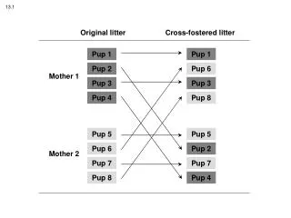
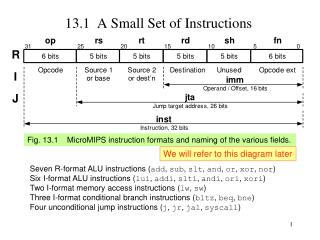
13.1 A Small Set of Instructions Fig. 13.1 MicroMIPS instruction formats and naming of the various fields. We will refer to this diagram later Seven R-format ALU instructions (add, sub, slt, and, or, xor, nor) Six I-format ALU instructions (lui, addi, slti, andi, ori, xori) Two I-format memory access instructions (lw, sw) Three I-format conditional branch instructions (bltz, beq, bne) Four unconditional jump instructions (j, jr, jal, syscall)
op 15 0 0 0 8 10 0 0 0 0 12 13 14 35 43 2 0 1 4 5 3 0 fn 32 34 42 36 37 38 39 8 12 Copy The MicroMIPS Instruction Set Arithmetic Logic Memory access Control transfer Table 13.1
13.2 The Instruction Execution Unit Fig. 13.2 Abstract view of the instruction execution unit for MicroMIPS. For naming of instruction fields, see Fig. 13.1.
13.3 A Single-Cycle Data Path Fig. 13.3 Key elements of the single-cycle MicroMIPS data path.
lui imm An ALU for MicroMIPS Fig. 10.19 A multifunction ALU with 8 control signals (2 for function class, 1 arithmetic, 3 shift, 2 logic) specifying the operation.
13.4 Branching and Jumping (PC)31:2 + 1 Default option (PC)31:2 + 1 + imm When instruction is branch and condition is met (PC)31:28 | jta When instruction is j or jal (rs)31:2 When the instruction is jr SysCallAddr Start address of an operating system routine Update options for PC Fig. 13.4 Next-address logic for MicroMIPS (see top part of Fig. 13.3).
13.5 Deriving the Control Signals Table 13.2 Control signals for the single-cycle MicroMIPS implementation. Reg file ALU Data cache Next addr
Control Signal Settings Table 13.3
Instruction Decoding Fig. 13.5 Instruction decoder for MicroMIPS built of two 6-to-64 decoders.
Control Signal Generation Auxiliary signals identifying instruction classes arithInst = addInst subInst sltInst addiInst sltiInst logicInst = andInst orInst xorInst norInst andiInst oriInst xoriInst immInst = luiInst addiInst sltiInst andiInst oriInst xoriInst Example logic expressions for control signals RegWrite = luiInst arithInst logicInst lwInst jalInst ALUSrc = immInst lwInst swInst AddSub = subInst sltInst sltiInst DataRead = lwInst PCSrc0 = jInst jalInst syscallInst
Fig. 10.19 Fig. 13.4 addInst Control subInst jInst . . . . . . sltInst Putting It All Together Fig. 13.3
13.6 Performance of the Single-Cycle Design Instruction access 2 ns Register read 1 ns ALU operation 2 ns Data cache access 2 ns Register write 1 ns Total 8 ns Single-cycle clock = 125 MHz R-type 44% 6 ns Load 24% 8 ns Store 12% 7 ns Branch 18% 5 ns Jump 2% 3 ns Weighted mean 6.36 ns Fig. 13.6 The MicroMIPS data path unfolded (by depicting the register write step as a separate block) so as to better visualize the critical-path latencies.