Download
1 / 31
320 likes | 474 Views
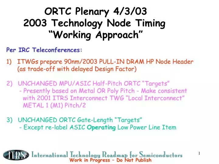
ORTC Plenary 4/3/03 2003 Technology Node Timing “Working Approach” Per IRC Teleconferences: ITWGs prepare 90nm/2003 PULL-IN DRAM HP Node Header (as trade-off with delayed Design Factor) 2) UNCHANGED MPU/ASIC Half-Pitch ORTC “Targets”

E N D
ORTC Plenary 4/3/03 • 2003 Technology Node Timing • “Working Approach” • Per IRC Teleconferences: • ITWGs prepare 90nm/2003 PULL-IN DRAM HP Node Header • (as trade-off with delayed Design Factor) • 2) UNCHANGED MPU/ASIC Half-Pitch ORTC “Targets” • - Presently based on Metal OR Poly Pitch - Make consistent • with 2001 ITRS Interconnect TWG “Local Interconnect” • METAL 1 (M1) Pitch/2 • 3) UNCHANGED ORTC Gate-Length “Targets” • - Except re-label ASIC Operating Low Power Line Item Work in Progress – Do Not Publish
Jan 2003 IRC 2003 ITRS Renewal ORTC Table Header/”Targets” “Working Approach”: 2003 ITRS Technology Node Header (90nm/2003 PULL-IN from 2001/2002 ITRS): Near-Term Long Term Notes ---------------------------------- --------------- ----- UNCHANGED: 2003 2004 2005 2006 2007 2008 2009 2012 2015 2018 DRAM HP WAS 100 90 80 70 65 57* 50* 35* 25* 18* (1) DRAM PULL-IN IS 90 80 70 65 57 50 45 32 22 16 (2) Other ORTC Tracked Technology Trends (optional - use by TWG Tables as needed): UNCHANGED: MPU/ASIC HP WAS 107 90 80 70 65 57* 50* 35* 25* 18* (3)*** UNCHANGED: MPU Pr GL WAS/IS: 65 53 45 40 35 32* 28* 20* 14* 10* (4) MPU Ph GL WAS/IS: 45 37 32 28 25 22* 20* 14* 10* 7* (5) Lo Oper.Pwr Pr GL 90 75 65 53 45 40* 36* 25* 18* 13* (6) Lo Oper.Pwr Ph GL 65 53 45 37 32 28* 25* 18* 13* 9* (7) * Not visible in 2001 ITRS due to no "annualized" columns between "Near Term" and "Long Term" column ranges. ** 90nm DRAM Half-Pitch pull-in from 2004 to 2003 to compensate for cell design factor push-out ***(Note 3) UNCHANGED, but need to Correlate Poly and “Metal 1” (M1) with IC TWG “Local Wiring”/2: 107/’03: 90nm/’04, then 3-year target cycle (parallelto DRAM HP); ** *** Work in Progress – Do Not Publish
Production Ramp-up Model and Technology Node 100M 200K Development Production 10M 5 20K 5 1M 1 2 3 4 2K Volume (Parts/Month) Alpha Tool Beta Tool Production Tool 100K Volume (Wafers/Month) 200 10K First Two Companies Reaching Production 20 First Conf. Papers 1K 2 0 12 24 -36 -24 -12 Months Source: 2001 ITRS - Exec. Summary Figure 2 5 5 1 2 3 4 Work in Progress – Do Not Publish
“Technology Node Solution” .35x = -65%/3yrs= 0.7071x/yr = .50x/2yrs Goal: [.71x/year] Hynix Confidential – ITRS Member Use Only Work in Progress – Do Not Publish DRAM Technology Roadmap • 2 year node by 90nm, then 3 year node • Keeping cell size scaling by -66% every 3 years
DRAM Cell Area History / 2001 ITRS Model ITRS 2003 “Working Approach”: 90nm/8F2 in 2003 (6F2/2005-12; 4F2 (red)/2013-2018) => Trends: 0.71/yr (-29%/yr)/thru ’07 then ~0.76 (-24%/yr) DRAM Cell Area Historical Actual <- > 2001 ITRS History <-- 2000 --> F'cast 10 1 Mb 0.35x / 3 Years –29%/yr (est.) CAF (A) Actual Scaling Acceleration, Or Equivalent Scaling Innovation is STILLNeeded to maintain historical trend = 31 = 31/1.0^2 29 (per 1 FEP) 4 Mb 16 Mb CAF (A) CAF (A) 64 Mb = 22 = = 16 = CAF (A) 11/.71^2 4.0/.5^2 = 11 = 26 (per 21 (per 1.3/.35^2; FEP) FEP) .71/.25^2 Cell Area (u2) 0.1 16->10 (per FEP) 128/256Mb 512Mb CAF (A) = 8.0 = DRAM Cell Size Historical Trend: Half-Pitch Scaling, contributed ~ .5x / 3 years [(.7x)^2] Cell Design innovation contributed additional ~ .7x / 3 years .35/.21^2; .26/.18^2 1Gb / 2Gb 10 -> 8 (per FEP) CAF (A) = 6 0.01 8 4Gb / 8Gb CAF (A) = 6 16Gb / 32Gb CAF (A) = 4 0.001 1986 1989 1992 1995 1998 2001 2004 2007 2010 2013 2016 6 64 Gb/128Gb Sources: Sematech, 2001 ITRS ORTC Year CAF (A) = 4 Work in Progress – Do Not Publish
Actual Scaling Acceleration, Or Equivalent Scaling InnovationNeeded to maintain historical trend ITRS 2001 “Moores Law” Targets: DRAM: 2x/2.5yrs; 1.05x/yr Chip Size MPU: 2x/node = 2x/3years; FLAT Chip Size Work in Progress – Do Not Publish Density Trends (bits/cm2, t/cm2) – ITRS / ORTC
MPU Clock Frequency Actual vs ITRS Historical <- > 1999 ITRS 2001 ITRS 100,000 2X / 4 Years 10,000 Actual Scaling Acceleration, Or Equivalent Scaling InnovationNeeded to maintain historical trend 1,000 Frequency (MHz) 2X / 2½ Years 100 MPU Clock Frequency Historical Trend: Gate Scaling, Transistor Design contributed ~ 17-19%/year Architectural Design innovation contributed additional ~ 21-13%/year 2X / 2 - 2½ Years 10 1 1980 1985 1990 1995 2000 2005 2010 2015 28 Sources: Sematech, 2001 ITRS ORTC Goal: Increase Speed by 2x Speed/2-2.5 years Work in Progress – Do Not Publish
Summary • “Technology Node Solution” : Pull-in 90nm to compensate for Cell Area Design Factor delay • Single “Working Approach” to focus all TWG work on the impact and potential solutions • Goal to reduce DRAM Cell Area in half every 2 years (double density/constant chip size) is not met after 2007, even with node pull-in • NO CHANGES to Logic Models for now – IRC still working on confusion over Logic “Node” definitions – need to consider both Half-pitch (density/chip size) and Gate Length (speed) goals
2003 IRC 2003 ITRS Renewal ORTC Table Header/”Targets” FINAL “Working Approach” (continued – additional NOTES/Comment details): Additional Notes/trend algorithms: (1) DRAM HP WAS: 3-year node cycle from 130nm/2001. (2) DRAM HP IS: 90nm PULL-IN to 2003, then 3-year node cycle from 2001; used as solution trade-off due to DRAM Cell Design Factor delay from WAS: 2001-2002/8; 2003-2010/6; 2011-2016/4(RED); to IS: 2003-2004/8; 2005-2010/6; 2011-2018/4(RED). (3) MPU/ASIC HP WAS/UNCHANGED: 2-yr node cycle to 90nm/2004, then 3-yr cycle parallel to DRAM HP; MPU/ASIC Half-Pitch was unchanged at the 2002 Update, but there were doubts that the ACTUAL MPU/ASIC Half-Pitch (un-contacted Poly or Metal) met the definition requirements for 10K units of process and customer qualified product from two companies within 3 months. With recent evidence from leading-edge manufacturers announcements and articles, the MPU/ASIC targets should remain UNCHANGED in the “MOST AGGRESSIVE” 2003 ITRS IRC case. The ORTC MPU/ASIC Poly and Metal 1 Half-Pitch numbers should be correlated for consistency to equal the Interconnect TWG ITRS "Local Wiring Pitch" line item numbers divided in half. (4)&(5) MPU High Performance Gate Lengths UNCHANGED: 2-yr node cycle to 2005, then 3-yr; (6)&(7) ASIC Low Operating Power Gate Lengths UNCHANGED: 2-yr delay from MPU Pr GL; however, PIDs proposal to rename to Low Operating Power; Add’l Notes: Only the NODE Header Line Item is standard for all TWG Tables: DRAM Half-Pitch (Size/Density-driven); other ORTC Technology Header line items are optional at TWG discreation; examples: 1) Physical GL (Performance-driven); 2) Low Operating Power GL (Power-driven) Work in Progress – Do Not Publish
Reasons for: “Working Approach ” • From IRC teleconferences: • Reasons for using ONLY the “Working Approach” of 90nm/2003 PULL-IN/8f2 PUSH-OUT: • The industry challenges, requirements, and solutions determined by the ITRS using the 2001 UNCHANGED timing have been explored over two consecutive years of work and are known; • Working with 2 sets of timing data until July will create confusion with already massive and detailed data. ITWGs tables contain data, dependent on other ITWG data, which has to be cross-checked among the ITWGs' teams. With a 2-scenario approach, and with July as the date to finalize the timing, ITWGs would have less than 8 weeks to reach worldwide consensus within their own groups and then respond to other ITWG work in order to produce a validated document by September in time for regional executive and advisory review. • Using ONLY the most aggressive scenario NOW focuses all groups on the details of the critical challenges, industry needs, and areas of no known solutions, identifies needed areas of innovation based on the 90nm timing pull-in, AND allows time for the critical cross-checks that occur among the various technologies. Work in Progress – Do Not Publish
The ITRS technology “Production Time Zero” refers to the first fully-qualified technology manufacturing ramp by one company, followed within 3 months by a second company. Furthermore, the terminology “fully-qualified" refers to the completion of both process and product qualification. Process qualification refers to a factory manufacturing status where there are no technical limitations to the beginning of product manufacturing ramp, and is usually achieved through the use of test vehicles (such as SRAM arrays, ring oscillators, DRAM arrays, and sometimes actual products). Product qualification refers to the approval by customers to ship product, after a period of quality and reliability testing of sample quantities of product from the “process-qualified” manufacturing line. For further clarification, a figure is included (attached foil/figure 2), which shows a typical timeline for: (1) delivery of Alpha Tool manufacturing equipment, typically 36 months before the “fully-qualified” “Time Zero”, and the completion of qualification of Alpha tools, typically within 12 months; and (2) delivery of Beta tool versions of the manufacturing equipment, typically 24 months prior to “Time Zero.” During the Beta Tool period, typically 24 to 12 months prior to fully qualified production, the equipment undergoes continuous improvement and qualification, along with materials and process flows. During the Beta period, the first conference papers (ISSCC, VLSI Symposium, IEDM, etc.) and industry articles appear. Beta tool, material, and process qualification must be completed before (3) release of a full-flow factory using qualified Production Tools to manufacture product qualification samples and risk production starts. That final period before fully-qualified production release is typically 12 months prior to “Time Zero,” but may be quite variable due to different customer quality and reliability testing requirements. This period is represented as a “gray box” rather than a continuous product quantity ramp, in the timeline figure 2. Nevertheless, it is expected that during this 12-month period the first leading-edge manufacturers will achieve the shipment of at least 10,000 fully qualified units from their manufacturing line (4). It is also expected that the subsequent ramps to very high volumes (Millions of units) will then occur, reaching a typical 10K-30K wafer-start-per-month fab capacity (5) within 12 months. This high ramp rate and utilization level after "Time Zero" will be dependent upon market and economic conditions that are prevalent once full qualification is reached. Foundry fabs are typically responsible only for process qualification and may receive small lot orders from several "fabless" customers which result in combined shipments of 10,000 units. CSTN Technology “Production Time Zero” Definition Proposal Work in Progress – Do Not Publish
Hynix Confidential – ITRS Member Use Only 2003 Roadmap : DRAM Work in Progress – Do Not Publish
Additional analysis per A.Allan, 3/03 Goal: .35x = -65%/3yrs = 0.7071x/yr = .50x/2yrs Hynix Confidential – ITRS Member Use Only 2003 Roadmap : DRAM Work in Progress – Do Not Publish
Additional analysis per A.Allan, 3/03 Goal: .35x = -65%/3yrs = 0.7071x/yr = .50x/2yrs 10 FERAM Cell Size Scaling Goal WAS: [’04-’07 0.71x/year ’07-’16 ave.76x/year] + FERAM[+ FLASH (TSIA Proposal)] DRAM Cell Size Scaling Goal WAS: [’99-’04 .71x/year ’04-’16 ave.765x/year] DRAM Cell Size Scaling Goal IS: [’99-’07 .71x/year ’07-’16-’?? ave.76x/year] FERAM Cell Size Scaling Goal IS: [’03-’07 0.71x/year ’04-’16-’?? ave.76x/year] ‘01 ‘04 ‘07 ‘10 ‘13 ‘16 ‘01 ‘03 ‘06 ‘09 ‘12 ‘15 ‘18 Hynix Confidential – ITRS Member Use Only Work in Progress – Do Not Publish 2003 Roadmap : DRAM
.77? Hynix Confidential – ITRS Member Use Only Additional analysis per A.Allan, 2/03 2003 Roadmap : FeRAM Work in Progress – Do Not Publish
[Additional analysis per A.Allan, 4/03] [ Flash HP “A” Factor?: 5.2 4.9 5.6 7.3 7.3 7.7 8.5 ] [ Flash Node “A” Factor?: 13 9.5 10 11 11 12 14 ] Source: TSIA Report - Jack Sun, TSMC, April 3, 2003 Flash Roadmap Proposal
90-nm Pull-in/6f2 Push-out DRAM Chip Size Model Impact Work in Progress – Do Not Publish
(Cell Array Area / Chip Size) x 100 = Cell Array Efficiency (%): Chip Size = (A x f 2 x Nbits)/CAE Cell Array Area = Cell Area x number of bits (2 n) f 2 Cell Area = Cell Area Factor (A) x f 2 ; f = technology node (half-pitch) feature size; Example: Cell Area = 2x4 x f 2 = 8 f 2 Chip Size Model Calculation Illustration - DRAM
90-nm Pull-in/6f2 Push-out DRAM Chip Size Model Impact – 2003 Roadmap Proposal Forecast: Work in Progress – Do Not Publish
90-nm Pull-in/6f2 Push-out DRAM Chip Size Model Impact – 2003 Roadmap Proposal Forecast: Work in Progress – Do Not Publish
90-nm Pull-in/6f2 Push-out DRAM Chip Size Model Impact – Historical SEMATECH Data: Work in Progress – Do Not Publish
90-nm Pull-in/6f2 Push-out DRAM Chip Size Model Impact – 2003 Roadmap Proposal Forecast: Work in Progress – Do Not Publish
90-nm Pull-in/6f2 Push-out DRAM Chip Size Model Impact – Original 2001/2002 ITRS UNCHANGED: Work in Progress – Do Not Publish
Elpida EDD5104ABTA-7A 512M DDR SDRAM Structural Analysis Manufacturer:Elpida • Part Number:EDD5104ABTA-7A • Device Type:512M DDR SDRAM • Date Code:0203 • Die Size:134.5 mm2 • The Elpida EDD5104ABTA-7A was manufactured in a 0.13 µm (0.09 µm minimum gates) full CMP, CMOS process with three levels of metal (tungsten Metal 1) and four levels of polysilicon. It uses Shallow Trench Isolation (STI) and twin wells in a P-substrate. • Design Features • Three metal device. Aluminum metals 3 and 2, Tungsten metal 1 • Sub-micron metal pitches at all levels • Metal 2 tungsten plugs as long as 3.55 microns • Tungsten metal 1 widths as thin as 0.075 micron • http://www.chipworks.com/reports/flyers/Elpida/Elpida_EDD5104ABTA_512M_DDR_SDRAM_SAR-0207-002.htm Chipworks 10/02 : Elpida 512Mb/130nm; EBN, 10/02: Hynix 512Mb/100nm Hynix rolls out 512-Mbit DDR based on 100-nm processEBN(10/29/02 04:25 p.m. EST) Hynix Semiconductor Inc. said it has developed 512Mbit DDR SDRAM manufactured with 0.10-micron technology. The new 512 Mb DDR SDRAM memory is aimed at PC and server products. The new product is compatible with DDR 266, DDR 333, and DDR 400, the company said. Hynix will implement the integrated design technology and manufacturing process in its plants in Ichon, Choongju, and Eugene, Oregon. Hynix is planning to launch mass production of 512Mb DDR SDRAM by the end of the year. Production of 256Mb and 1Gb DDR SDRAM using 0.10-micron technology will occur in the first half of next year, it said. http://www.siliconstrategies.com/story/OEG20021029S0030 Work in Progress – Do Not Publish
Logic Model Work in Progress – Do Not Publish
MPU Chip size (mm2) – Historical Trends vs 2001 ITRS Model* 2003 ITRS Update – (No Changes from 2001 ITRS) 1000 800mm2 Litho Field Size 286mm2 2 per Field Size 572mm2 Litho Field Size HP MPU 310mm2 CP MPU 140mm2 100 CP Shrink 70mm2 *1999 Leading-Edge .18u CP MPU: 512KB (28Mt [58.3%] x 1.18u2/t = 34mm2) + 20Mt Logic x 5.19u2/t = 104mm2 + 2mm2 OH= 140mm2 = Total 48Mt x ave 2.92u2/t = 140mm2 *1999 Leading- Edge .18u HP MPU: 2MB (113Mt [81.9%] x 1.18u2/t = 135mm2) + 25Mt Logic x 5.19u2/t = 130mm2 + 45mm2 OH= 310mm2 = Total 138Mt x ave 2.25u2/t = 310mm2 * ITRS Design TWG MPU Transistors/Chip Model: ~2x/Node = 2x/2yrs from 1999 - 2001; then 2x/3yrs from 2001- 2016 10 1980 1985 1990 1995 2000 2005 2010 2015 2020 Goal: flat chip, reduce the size of SRAM cell and Logic Gate by 0.5x/2yrs (2x Functions /chip per 2yrs) CP MPU Intro 280mm2 1999 :6 x 1.18 = 7.08u2 per 6t (average) SRAM cell x .63 area efficiency = 4.46u2 = 137f2(cell) 4 x 5.19 = 20.8u2 per 4t (average) Logic Gate x .50 area efficiency = 10.4u2 = 320f2(gate)
Table numbers in nm, unless noted information based on publications / conferences / press releases / websites 120? 110 107 45 ‘03 Data added (blue) by M.Yoshimi (IRC Japan) to Dr.Arden’s original table, at 06.17.2002 Logic Technologies Characteristics of IC Vendors / Foundries for 130 / 90 nm nodes as compared to ITRS 2000 / 2001 Work in Progress – Do Not Publish Industry Data – Leading-Edge MPU/ASIC
Table numbers in nm, unless noted information based on publications / conferences / press releases / websites ? Data added (blue) by M.Yoshimi (IRC Japan) to Dr.Arden’s original table, at 06.17.2002 Logic Technologies Characteristics of IC Vendors / Foundries for 130 / 90 nm nodes as compared to ITRS 2000 / 2001 Work in Progress – Do Not Publish Industry Data – Leading-Edge MPU/ASIC, cont.
For the Business and Trade Press: INFXX200211.021e; Media Relations Contact: Worldwide Headquarters/U.S.A.; Asia; Japan - Name: Ralph Heinrich, Leslie Davis, Kaye Lim, Hirotaka Shiroguchi Investor Relations: Phone / Fax: +49 89 234 22404 / 28482; +1 408 501-6790 / 2424; +65 6840 0689 / 0073; +81 3 5449 6795 / 6401; +49 89 234 26655 / 26155 Email: alph.heinrich@infineon.com; leslie.davis@infineon.com; kaye.lim@infineon.com; hirotaka.shiroguchi@infineon.com; investor.relations@infineon.com Joint News Release by Infineon and Nanya Infineon and Nanya Seal DRAM Cooperation by Founding Production Joint Venture and Agreeing Technology Development Collaboration Munich/Germany and Taoyuen/Taiwan, November 13, 2002 – Infineon Technologies (FSE/NYSE: IFX), Munich, and Nanya Technology Corporation (NTC), Taoyuen/Taiwan, have signed final contracts concerning strategic cooperation on standard memory chips (DRAMs). The cooperation will help each partner expand its position in the DRAM market while sharing development costs. The agreement provides for the joint development of advanced 0.09-micron and 0.07-micron production technologies for 300mm wafers. Under the terms of the agreement the companies have also set up a 50:50 joint venture for the production of DRAM chips and will build a new joint 300mm facility in Taiwan. This facility will employ the production technology devel-oped jointly by the companies. Maximum production capacity will approach 50,000 wafer starts a month once the facility is fully operational. Initial production of the first 300mm wafers in the new facility is expected in late 2003. The new 300mm semiconductor facility will be constructed in two stages aligned with the growth and development of the world semiconductor market. The first stage, which is scheduled for completion in the second half of 2004, will give the facility an initial monthly capacity of around 20,000 wafer starts. Completion of the second stage, currently anticipated for mid-2006, will increase capacity to around 50,000 wafer starts a month, making the new semiconductor facility one of the world’s largest. The total investment planned in the next three years amounts to around Euro 2.2 billion. Infineon and Nanya will each invest Euro 550 million in their innova-tive memory chip production project until 2005, the lion’s share of which will be used to ramp up production in 2004 and 2005. When operating at maximum capacity, the facility will create up to 1,300 new jobs in Taiwan. The joint venture will be headquartered in Taoyuen/Taiwan, close to Nanya’s [- 2 -] existing production site. Subject to approval by the antitrust authorities, the joint venture will commence business operations on December 2, 2002. “This strategic partnership in the Asian growth market successfully extends our offensive in the worldwide market for memory chips and we are expanding our position as one of the three best semiconductor manufacturers”, explains Dr. Ulrich Schumacher, President and CEO of Infineon Technologies AG. “This cost-efficient way of boosting production capacities will also help us capture new business and drive our share of the global DRAM market up beyond the 20 percent mark.” “This partnership between our companies brings together our strengths, and allows Nanya to achieve it’s objective of being a highly competitive major supplier world-wide”, observed Dr. Jih Lien, President of Nanya Technologies. “We believe that this additional capacity will move Nanya to the number four ranking of DRAM makers with double digit market share.” New production technology, jointly developed at Infineon’s Dresden site, will be used in both companies and by the new joint venture. Further collaboration on the devel-opment of 0.09-micron and 0.07-micron reference products in Munich is also planned. Infineon and Nanya will between them commit more than 120 people to the development projects. The first 300mm wafer memory products using the new 0.09-micron process will leave the production line in late 2003. Plans are also in place to transfer the 0.09-micron production technology to 200mm wafers. Infineon has already begun technical preparations for 0.09-micron production. This November, for example, it produced the first demonstrators featuring a new cell design and new materials. The partners are developing the new production technology in concert using Infineon’s advanced DRAM trench technology for 300mm wafers, which the company licenses to Nanya, as a starting point. The switch to the smaller 0.09-micron and 0.07-micron geometries in chip design coupled with the outstanding area efficiency and high capacity of the trench technology will further enhance productivity. The new joint venture in Taoyuen will join Infineon’s international network of DRAM production sites. The global integration of Infineon’s memory facilities ensures [- 3 -] uniformly high levels of quality standards at all sites worldwide and a constant exchange of know-how and experience. About Nanya: Nanya Technology Corporation was officially founded on March 4, 1995. Set up to conduct research and development, design, manufacture, and sales of semi-conductor products, the company is headed by Mr. Y.C. Wang as the Chairman of the Board. The main shareholder is Nanya Plastics Corporations of the Formosa Plastics Group. Nanya started semiconductor production in 1996 and opened its North American branch company in San Jose, California, in 1997. The company began providing foundry services in 1997. For more information, please contact Nanya Technology Corporation at 408/441-7819. For headquarters in Taiwan, please call 886-3-328-1688 or visit the web site http://www.nanya.com. About Infineon: Infineon Technologies AG, Munich, Germany, offers semiconductor and system solutions for the automotive and industrial sectors, for applications in the wired communications markets, secure mobile solutions as well as memory products. With a global presence, Infineon operates in the US from San Jose, CA, in the Asia-Pacific region from Singapore and in Japan from Tokyo. In the fiscal year 2002 (ending Sep-tember), the company achieved sales of Euro 5.21 billion with about 30,400 employees worldwide. Infineon is listed on the DAX index of the Frankfurt Stock Exchange and on the New York Stock Exchange (ticker symbol: IFX). Further information is available at www.infineon.com. This news release is available at www.infineon.com/news. Contact at Nanya Technology Corporation: Charles Kau/Executive Vice President; Tel. +886-3-328-1688; Fax +886-3-396-0993; charleskau@ntc.com.tw Infineon/Nanya/Taiwan 90nm/70nm/300mm/2004-06/Production Announcement Work in Progress – Do Not Publish
Toshiba to Mass-Produce World's Smallest Chips By KANJI ISHIBASHI [Source:]DOW JONES NEWSWIRES TOKYO -- Toshiba Corp. plans to begin this spring mass production of the world's smallest semiconductors with circuit widths of 90 nanometers. The launch will come well ahead of the Japanese technology company's global rivals. The semiconductors will be much smaller than conventional 130-nanometer chips, allowing a significant boost to processing speeds and savings in energy consumption. The move underscores Toshiba's aim to lead the industry in cutting-edge chip process technology, a company spokesman said Thursday. "We would like to launch the fastest system LSIs [large-scale integrated circuits] in the market" ahead of other makers, he said. Toshiba's new 90-nanometer system chips will be embedded with dynamic random access memory, or DRAM, the company said. Toshiba plans to produce the new chips at its plant in Oita, southern Japan. The chips will be used for digital consumer electronics and game devices, the company said. The world's top two chip makers -- Intel Corp. of the U.S. and SamsungElectronics Co. of South Korea -- are slated to start mass-production of 90-nanometer chips this summer. NEC Electronics Corp., a new semiconductor unit of NEC Corp., said Thursday it plans to begin mass-producing 90-nanometer chips in the July-September quarter in Kanagawa Prefecture, west of Tokyo. Write to Kanji Ishibashi of kanji.ishibashi@dowjones.com <mailto:kanji.ishibashi@dowjones.com> Updated January 8, 2003 11:58 p.m. EST Recent 90-nm Technology Mfg Claims from Dow Jones NW 1/8/2003: Work in Progress – Do Not Publish