Download
1 / 7
70 likes | 146 Views
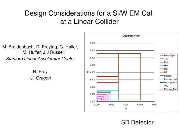
Design Considerations for a Si/W EM Cal. at a Linear Collider. M. Breidenbach, D. Freytag, G. Haller, M. Huffer, J.J Russell Stanford Linear Accelerator Center R. Frey U. Oregon. SD Detector.

E N D
Design Considerations for a Si/W EM Cal.at a Linear Collider M. Breidenbach, D. Freytag, G. Haller, M. Huffer, J.J Russell Stanford Linear Accelerator Center R. Frey U. Oregon SD Detector
SD designed for excellent energy flow performance – with well-understood and somewhat constrained cost (see Snowmass Orange Book for details) • Si/W ECal • 5mm transverse segmentation • [ 2.5 mm W (0.7 X0), 0.4 mm Si ] x30 • Rm = 9mm (1 + gap(mm)/2.5) → Keep gaps small ! In this talk: • Some architecture and readout issues • Dynamic range and some electronics issues • Next steps
Si/W Readout-SD • ~50 M pixels, 5x5 mm2 • Do NOT scale electronics by this number • 1 chip per wafer • 1 chip per ~1 m2 of wafers
Noise • GLAST Si electronics: 20e/pF + 200e →≈2000e (fine) Cooling • NLC duty cycle is ~10-4 → Assume 10-3 power duty cycle • GLAST elec. power: 2 mW/chan. • For standard W alloy, can cool one edge of W plate → ≈ 2o rise (fine) Dynamic Range • MIPs • 500 GeV Bhabha electrons • EGS study: ≈ 2000 MIPs • Maintain low-end resolution → 3 ranges of 12 bits
G1 M U X 12 bit A/D Shaper G2 G3 • Charge amp. with ~ 10pf feedback cap. • 3 ranges @ 12 bits
Next… • Further design work • Prototypes: • Silicon wafer with 5mm pixels and metallizations for wafer readout chip • Wafer readout chip • The other readout chips • A one wafer wide, full depth module for test beam