Download
1 / 19
190 likes | 285 Views
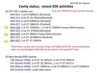
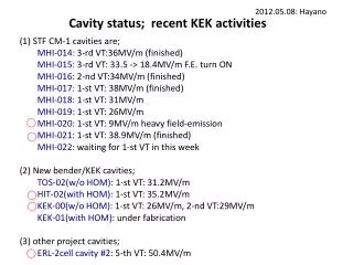
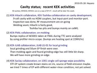
Recent Electron-Cloud Mitigation Studies at KEK. E-cloud mitigation mini-workshop on 20-21 November at CERN Kyo Shibata (for KEKB Group). Introduction. KEKB : double ring collider with one collision point. High Energy Ring (HER) : Electron ring

E N D
Recent Electron-Cloud Mitigation Studies at KEK E-cloud mitigation mini-workshop on 20-21 November at CERN Kyo Shibata (for KEKB Group)
Introduction KEKB : double ring collider with one collision point High Energy Ring (HER) : Electron ring Energy : 8 GeV, Current : 970 mA, bunch space : 36 ns, bunch charge : 0.910-8 C Low Energy Ring (LER) : Positron ring Energy : 3.5 GeV, Current : 1600 mA, bunch space : 36 ns, bunch charge : 1.210-8 C e+ Belle Detector Wiggler E-cloud study items at LER e- Clearing electrode RFA in Q-mag Groove surface clearing electrode groove surface TiN coating Wiggler Graphitization RFA type electron detectors TiN (antechamber) TiN, Graphitization Beam duct with antechambers and so on… RFA in solenoid Circumference : 3016 m 1 E-cloud mitigation mini-workshop on 20-21 November at CERN
Clearing Electrode 1 Mitigation of E-cloud in Magnets Clearing electrode and electron detector was installed in Wiggler magnet. (placed at the center of pole) To ascertain the effect of electrode, the electron density was measured from just under electrode. Tolerance for high beam current was also tested. Wiggler magnet Magnetic filed : 0.77 T Effective length : 346 mm Aperture (height) : 110 mm Clearing electrode Y. Suetsugu, ILCDR2008 Electron detector Test chamber 2 E-cloud mitigation mini-workshop on 20-21 November at CERN
Clearing Electrode 2 Cross-section Drawing Very thin electrode (0.1 mm, Tungsten) and insulator (0.2 mm, Al2O3) were developed. 7 strips measure the horizontal spatial distribution of the e-cloud. Collector (7 strips, w5 mm) Grid (~ 1 kV) Shield Monitor Block f2 mm holes R47 Limited by magnet aperture Beam Electrode [W] (~ +1 kV) Cooling channel (w40, l440, t~0.1) Insulator [Al2O3] (t~0.2 mm) Electrode Block Cooling Water paths Y. Suetsugu, ILCDR2008 Vacuum seal by metal O-ring 3 E-cloud mitigation mini-workshop on 20-21 November at CERN
Clearing Electrode 3 Top view & side view Magnet Top view Detachable Block Electron Monitor Block Side view Electrode Block Feed-through 5 Y. Suetsugu, ILCDR2008 4 E-cloud mitigation mini-workshop on 20-21 November at CERN
Clearing Electrode 4 Results Drastic decrease in electron density was demonstrated by applying positive voltage. Vr = 1.0 kV B = 0.77 T [Logarithmic scale] Vr = 0 V B = 0.77 T [Logarithmic scale] Velec [V] Velec [V] 1 x 10⁻⁵ Ie [A] 1 x 10⁻⁶ Ie [A] 1 x 10⁻⁷ 1585 bunches (Bs ~ 6 ns) ~1600 mA 1 x 10⁻⁸ 1 x 10⁻⁹ Collectors Collectors Y. Suetsugu, ILCDR2008 5 E-cloud mitigation mini-workshop on 20-21 November at CERN
Groove surface (preliminary) Effect of groove surface will be ascertained this autumn. (collaboration with SLAC) Flat surface [SUS + TiN] Electrode will be replaced by groove surface. Same setup for clearing electrode is utilized. Groove structure was designed and manufactured in SLAC. Flat surface with TiN coating is now tested for reference. TiN~200 nm Y. Suetsugu, ILCDR2008 TiN~50 nm [Groove] R47 Magnetic field Beam [Monitor] Groove surface [SUS + TiN] 6 E-cloud mitigation mini-workshop on 20-21 November at CERN
TiN coating 1 Reduction of SEY of beam duct by coating TiN coating system for long beam ducts was built at KEK. Gas inlet Coating was done by DC magnetron sputtering of titanium in Ar and N2. Solenoid Thickness : 200 nm ~4 m Maximum SEY of TiN film on sample piece was 0.84 (electron dose : 0.001 C/mm2) Several beam ducts have been coated with TiN, and installed in KEKB LER. Duct TiN coated Uncoated Pumping system K. Shibata, EPAC2008 7 E-cloud mitigation mini-workshop on 20-21 November at CERN
TiN coating 2 Measurement of electron density in KEKB f 94 mm Electron density in circular beam duct (94 mm) Electron Microscope Image K. Kanazawa Copper TiN (KEK) TiN (KEK) TiN (BNL) TiN (BNL) H. Hisamatsu and M. Nishiwaki 8 E-cloud mitigation mini-workshop on 20-21 November at CERN
TiN coating 3 Measurement of electron density in KEKB Electron density in beam duct with antechambers f 90 mm Y. Suetsugu, ILCDR2008 Combination of beam duct with antechambers and TiN coating is a promising candidate for future high current machines. 9 E-cloud mitigation mini-workshop on 20-21 November at CERN
Electron Gun Graphitization 1 Electron beam induced graphitization is also studied. Graphitized surfaces have shown low SEY in laboratory experiments. Maximum SEY decreased to 1.0-1.1 (electron irradiated : 0.0016 C/mm2) Setup for graphitization of copper beam duct was newly developed. 500 eV electrons irradiate to duct surface. Copper Duct 1.35m Emission Current Density : 170mA/cm2 Sample Piece Filament M. Nishiwaki and S. Kato, Vasscaa4 2008 10 E-cloud mitigation mini-workshop on 20-21 November at CERN
Graphitization 2 Measurement of electron density in KEKB Graphitization is effective to reduce electron cloud density. Effect is less than TiN and NEG. M. Nishiwaki and S. Kato, Vasscaa4 2008 [4.200.3] Graphite layer was too thin (FWHM 10 nm). Thicker carbon coating on copper duct is in preparation. 11 E-cloud mitigation mini-workshop on 20-21 November at CERN
Near Beam Electron Cloud Density Measurement in Magnetic Filed with RFA 1 Measurement of electron density in solenoid coil Only high energy electrons produced near the bunch can enter the groove and reach the detector behind it. With the help of simulation detector current is converted into the density near the beam. K. Kanazawa and H. Fukuma Starting points of electrons that enter the detector Groove +15 Detector 1 • Bunch size: x = 0.434mm, sy = 0.061mm, sz = 6mm, B = 50 G, NB = 7.51010 SR 0 y[mm] Beam Only these electrons reach the detector. Detector 2 Detector -15 Monitor used with solenoid field Monitor used without solenoid field -15 0 +15 x[mm] 12 E-cloud mitigation mini-workshop on 20-21 November at CERN
Near Beam Electron Cloud Density Measurement in Magnetic Filed with RFA 2 Groove Inside of the chamber 13 E-cloud mitigation mini-workshop on 20-21 November at CERN
Near Beam Electron Cloud Density Measurement in Magnetic Filed with RFA 3 Electron cloud density with solenoid field (B = 50 G) (0.005 T) B=0 Preliminary result B=50 G, Detector 2 B=50 G, Detector 1 K. Kanazawa and H. Fukuma The difference in two detectors may be due to ; • 1) COD • 2) Relative position to the primary synchrotron radiation • 3) Output offset of amplifier in measurement system. The measured current in a solenoid field might have included electrons drifting along the wall. 14 E-cloud mitigation mini-workshop on 20-21 November at CERN
Near Beam Electron Cloud Density Measurement in Magnetic Filed with RFA 4 Measurement of electron density in Q-magnet Electrons accelerated by a bunch along X-axis reach the detector. Electrons accelerated with small angle to X-axis moves spirally around X-axis losing their energy along X-axis to the spiral motion. Electrons with sufficient energy and direction close to X-axis reach the detector. With the help of simulation detector current is converted into the density near the beam. x = 0.35 mm, y = 0.094 mm, z = 6.0 mm, B’ = 3.32 T/m, NB = 7.51010 K. Kanazawa and H. Fukuma +20 Detector Bias = -1 keV X-axis Detector Detector Detector 2 0 x [mm] SR The big island is an expected source. Other small islands are unexpected. Detector 1 -20 -20 0 20 y [mm] 15 E-cloud mitigation mini-workshop on 20-21 November at CERN
Near Beam Electron Cloud Density Measurement in Magnetic Filed with RFA 5 Detector 16 E-cloud mitigation mini-workshop on 20-21 November at CERN
Near Beam Electron Cloud Density Measurement in Magnetic Filed with RFA 6 Electron cloud density with quadrupole field (B’ = 3.32 T/m) Preliminary result K. Kanazawa and H. Fukuma The difference in two detectors may be due to ; • 1) COD • 2) Relative position to the primary synchrotron radiation • 3) Output offset of amplifier in measurement system. The observed value in Q-Magnet is close to the estimation by simulation 17 E-cloud mitigation mini-workshop on 20-21 November at CERN
Summary Various studies on the electron cloud mitigation have been done at KEKB positron ring. Clearing electrode Groove surface TiN coating Graphitization Beam duct with antechambers Mitigation methods, such as clearing electrode and coating gave reasonable effect. New RFA type electron detectors was developed and installed in KEKB LER to measure the electron cloud density in solenoid coil and quadrupole magnet. For SuperKEKB : Drift space : antechamber + solenoid + TiN coating Magnet space: antechamber + TiN coating + clearing electrode? groove surface? 18 E-cloud mitigation mini-workshop on 20-21 November at CERN