Download
1 / 2
20 likes | 209 Views
Low-Voltage Nanodomain Writing in He-Implanted Lithium Niobate Crystals Richard M. Osgood, Columbia University, DMR 0806682.

E N D
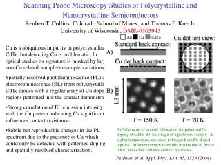
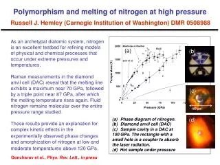
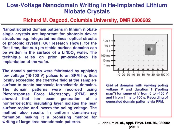
Low-Voltage Nanodomain Writing in He-Implanted Lithium Niobate CrystalsRichard M. Osgood, Columbia University, DMR 0806682 Nanostructured domain patterns in lithium niobate single crystals are important for photonic device structures e.g. integrated nonlinear optical circuits or photonic crystals. Our research shows, for the first time, that sub-µm stable surface domains can be written in the surface of a LiNbO3 wafer. The technique relies on prior µm-scale-deep He implantation of the wafer. The domain patterns were fabricated by applying low voltage (10-100 V) pulses to an SPM tip, thus locally exceeding the coercive field at the sample’s surface to create nanoscale ferroelectric domains. The domain patterns were recorded using Piezoresponse Force Microscopy (PFM) and showed that ion beam generation of a nonferroelectric insulating layer isolates the near surface region and lowers the poling voltage. The method also results in uniform domain-array formation, making it a promising method for writing of large-area nanodomain patterns. Grid of domains with varying poling voltage V and duration t (“poling map”) for range of V from 0 to +100 V and t from 1 ms to 100 s. Recording of generated domain patterns via PFM. Lilienblum et. al., Appl. Phys. Lett. 96, 082902 (2010)
Patterning and Fabrication of NanostructuredMetallodielectric Crystals Richard M. Osgood, Columbia University, DMR 0806682 Our Materials World Network has had many broad impacts. But one of the most important has been to draw together a powerful highly diverse international interdisci-plinary team. Our team has involved a German professor and her student at the University of Bonn, two strong groups at BNL using X-ray measurements and theory (Ken Evans-Lutterodt and Dave Welch), respectively, and our UK theoretician, NicolaePanoiu, and Dr. Marko Kralj, a Croatian Physicist, Our team has also involved a several US REU students and a Ethiopian female summer student. These aspects have provided our Materials students a rich educational environment. Columbia Materials World Network Overseas Team Members Dr. Ken Evans-Lutterodt Dr. Marko Kralj Prof. NicolaePanoiu Prof. Elisabeth Soergel

![[1] J. Zhang et al. , Appl. Phys. Lett . 88 , 123112 (2006).](https://cdn2.slideserve.com/3783086/slide1-dt.jpg)