Download
1 / 37
410 likes | 625 Views
Design of Capacitive Displacement Sensors for Chip Alignment. Jose Medina Professor N. McGruer. Outline. Introduction Displacement sensors Capacitive sensors FEM simulations Readout circuit Scaled models Experiments Conclusions. Introduction. Approach Assemble Alignment Transfer.

E N D
Design of Capacitive Displacement Sensors for Chip Alignment Jose Medina Professor N. McGruer
Outline • Introduction • Displacement sensors • Capacitive sensors • FEM simulations • Readout circuit • Scaled models • Experiments • Conclusions
Introduction Approach • Assemble • Alignment • Transfer 2
Introduction • Requirements • Accuracy to nm • Cost effective • Fast • Compatible • Fabrication • Electronics • Actuator (nanopositioner) • Variable gap • Connections to only one side
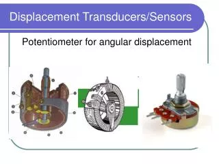
Displacement Sensors A. A. Kuijpers, ‘Micromachined Capacitive Ling-Range Displacement Sensor for Nano-positioning of Microactuator Systems’, PhD thesis, Universiteit Twente
Capacitive sensors Capacitive sensor literature • Widely used • Drug delivery, temperature/humidity sensors, automotive, positioners • No sensor moves in two dimensions ‘Modeling and Optimization of a Fast Response Capacitive Humidity Sensor’, Tetelin ‘Perspectives on MEMS in Bioengineering: A Novel Capacitive Position Microsensor’, Pedrocci
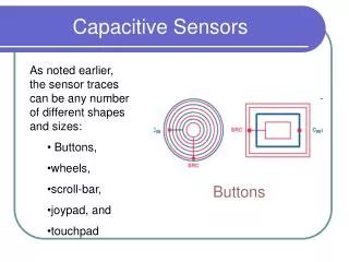
Capacitive sensors Electrodes on substrate and template
Capacitive sensor ~ C=Q/V=f(geometry) Chip alignment: connections only on one electrode
Capacitive sensor Complete system Equivalent circuit
Capacitive sensor Cantor set geometry • First level • Second level • Third level
Capacitive sensor Central fractal geometry • First level • Second level • Third level
FEM simulations Numerical method A. Hiekes, SIEMENS; Baxter, Capacitive Sensors
FEM simulations Modeling scenarios • Closed system • Open boundary • Natural boundary condition • Trefftz domain • Infinite elements ANSYS, Inc
FEM Simulations Models • Doped Si substrates • Glass top substrate • Glass bottom substrate
Readout Circuit Converter • transforms a signal to another more convenient Voltage applied at capacitor
Readout circuit Alignment precision and converter performance Circuits • Oscillator • AC-bridge • Transimpedance amplifier • Switched-capacitor • Sigma-Delta modulator
Readout circuit Transimpedance amplifier Synchronous demodulator Low pass filter
Readout circuit φ1 φ2 Switched-Capacitor Amplifier
Readout circuit Sigma-Delta modulator Cap-to-digital converter based on SC modulator
Scaled Models Scaled models • How do and C scale with geometry?
Scaled Models Theoretical accuracy Scaled models
Experiments Two PCBs • Large w/g ratio • Max accuracy? • Small w/g ratio • Geometry performance?
Experiments Setup • Stage • PCBs • Readout circuit • AD7745 • Connectors, wires • Computer
Experiments Results: large feature board • Experiments greater capacitance • Sim and experiments same profile • Experiments different results • Accuracy • 5fF (specs 4fF) • 0.1mm (calculations 2 μm) • Sim/exp results further for long displacements
Experiments Results: small feature board • Cap increases with displacement! • Similar profiles • Good performance at short gap • Min largest gap 3mm (u=0.762 mm)
Conclusions Simulations • DC capacitance • Ground close than at infinite • 5 electrodes + stage • Sim/exp further for large gaps • Cap to stage dominant • Variations between experiments • Plates not parallel, gap varies • Increase cap with displacement • C13 and C23 decrease • C12 dominant, board ‘perturbs’ E
Conclusions Sensor design suggestion • Central fractal geometry • Width depends upon min/max gap • Min: g/w < 1/3 for last level to take over, ideally <1/10 • Max: g/w < 1 to avoid instabilities • Capacitor width w, #levels u • Chip 15x15 mm sq sensor 0.5x0.5 mm sq
Thank you for you attention Acknowledgments • Advisor: Professor McGruer • Professors: Adams, Busnaina, Muftu, Papageorgious, Sun • Students: Prashanth, Juan Carlos Aceros, Peter Ryan, Andy Pamp, Siva, Harris Mussolis
Capacitive sensors Definition Capacitance Conductor a + + + + + + + + + + + + e- + + + + + + + + + + + + + + + + + + + + + + + + + + + + + Vs - - - - - - - - - - - - - - - - - - - - - - - - - - - - - Conductor b
FEM Simulations Convergence
Switched-Capacitor amplifier φ1 φ2 • Charge-transfer phase (φ1 off, φ2 on) • Sampling phase (φ1 on, φ2 off)
Correlated Double Sampling • Processing phase • Sampling phase
Simulations switched-capacitors V (volts) Time (ms)