Download
1 / 27
270 likes | 429 Views
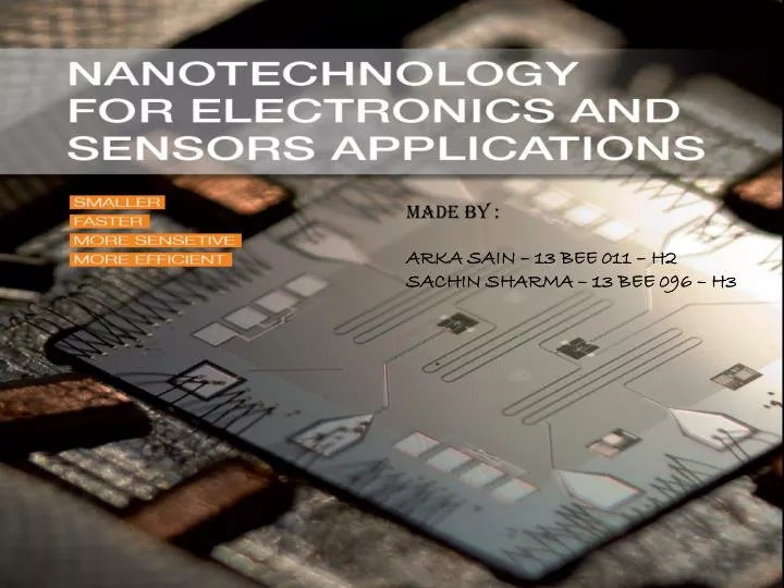
MADE BY : ARKA SAIN – 13 BEE 011 – H2 SACHIN SHARMA – 13 BEE 096 – H3. WHAT IS NANOTECHNOLOGY?.

E N D
MADE BY : ARKA SAIN – 13 BEE 011 – H2 SACHIN SHARMA – 13 BEE 096 – H3
WHAT IS NANOTECHNOLOGY? Nanotechnology is the understanding and control of matter and processes at the nanoscale, typically, but not exclusively, below 100 nanometres in one or more dimensions where the onset of size-dependent phenomena usually enables novel applications. Nanotechnology is cross-disciplinary in nature, drawing on medicine, chemistry, biology, physics and materials science.
At the nanoscale, matter begins to demonstrate entirely new and unique properties. It can become stronger, conduct heat better, and show extraordinary electrical properties. • With a bottom-up approach, nanostructures are formed molecule by molecule, using methods such as chemical vapour deposition or self-assembly. By contrast, top-down fabrication can be likened to sculpting from a base material, and typically involves steps such as deposition of thin films, patterning, and etching.
Bottom ⇨ Up: • Building what you want by assembling it from building blocks ( such as atoms and molecules). • Atom-by-atom, molecule-by-molecule, or cluster-by-cluster Two Different Approaches to Nanofabrication • Top ⇨ Down: • Start with the bulk material and “cut away material” to make what you want
Why nanotechnologyMatters ? The advances in nanotechnology have brought new tools to the field of electronics and sensors. New designed materials offer new and unique properties enabling the development and cost efficient production of state-of-the-art components that ::: Operate Faster Higher Sensitivity Consume Less Power Can be packed at much higher densities
Numerous products based on nanotechnology have been reaching the market for some years, all the way to end users and consumers. For instance, at the nanoscale, the resistance dependence of a material on an external magnetic field is significantly amplified, which has led to the fabrication of hard disks with a data storage density in the gigabyte and terabyte ranges. Nanotechnology has also enabled the development of sensors suitable for measurements at the molecular level with an unprecedented sensitivity and response time, mainly due to their high surface to volume ratio.
CARBON-BASED SENSORS AND ELECTRONICS The semiconductor industry has been able to improve the performance of electronic systems for more than four decades by downscaling silicon-based devices but this approach will soon encounter its physical and technical limits. This fact, together with increasing requirements for performance, functionality, cost, and portability have been driven the microelectronics industry towards the nano world and the search for alternative materials to replace silicon.
Carbon nanomaterials such as one-dimensional (1D) carbon nanotubes and two-dimensional (2D) graphene have emerged as promising options due to their superior electrical properties which allow for fabrication of faster and more power-efficient electronics. • At the same time their high surface to volume ratio combined with their excellent mechanical properties has rendered them a robust and highly sensitive building block for nanosensors.
Graphene transistor In 2004, it was shown for the first time that a single sheet of carbon atoms packed in a honeycomb crystal lattice can be isolated from graphite and is stable at room temperature. The new nanomaterial, which is called graphene, allows electrons to move at an extraordinarily high speed. This property, together with its intrinsic nature of being one-atom-thick, can be exploited to fabricate field-effect transistors that are faster and smaller. A layer of graphene acts as the conducting channel in a field-effect transistor.
When a layer of graphene is rolled into a tube, a single-walled carbon nanotube (SWNT) is formed. • Consequently, SWNTs inherit the attractive electronic properties of graphene but their cylindrical structure makes them a more readily available option for forming the channel in field-effect transistors. • Such transistors possess an electron mobility superior to their silicon-based counterpart and allow for larger current densities while dissipating the heat generated from their operation more efficiently. • During the last decade, carbon nanotube-based devices have advanced beyond single transistors to include more complex systems such as logic gates and radio-frequency components. Carbon nanotube electronics
Carbon-based nanosensors • In addition to the exceptional electrical properties of graphene and carbon nanotubes, their excellent thermal conductivity, high mechanical robustness, and very large surface to volume ratio make them superior materials for fabrication of electromechanical and electrochemical sensors with higher sensitivities, lower limits of detection, and faster response time. • A good example is the carbon nanotube-based mass sensor that can detect changes in mass caused by a single gold atom adsorbing on its surface.
An artistic expression of an integrated circuit based on individual carbon nanotubes.
Any additional gold atom that adsorbs on the surface of a vibrating carbon nanotube would change its resonance frequency which is further detected.
MOLECULAR ELECTRONICS Recent advances in nanofabrication techniques have provided the opportunity to use single molecules, or a tiny assembly of them, as the main building blocks of an electronic circuit. This, combined with the developed tools of molecular synthesis to engineer basic properties of molecules, has enabled the realization of novel functionalities beyond the scope of traditional solid state devices.
Single Molecule Memory Device • A modern memory device, in its most common implementation, stores each bit of data by charging up a tiny capacitor. • The continuous downscaling of electronic circuits, in this context, translates to storing less charge in a smaller capacitor. • Ultimately, as memory device dimensions approach the nanometer range, the capacitor can be replaced by a single organic molecule such as Ferrocene, whose oxidation state can be altered by moving an electron into or out of the molecule.
Organic field-effect transistors (OFETs) are a good example of the scope of traditional electronic devices being augmented by the chemical reactivity of an organic semiconductor material in their channel. In an odour sensor, for instance, the nano-scale chemical reactions upon exposure of the device to a certain atmospheric condition modify the electronic properties of the organic semiconducting material which is further reflected by a change in the current flowing through the transistor. Organic Transistor Odour Sensor
QUANTUM COMPUTING Quantum computing chip: the two black squares are the quantum bits or qubits, the processing centre; the meandering line at the centre is the quantum bus; and the lateral meandering lines are the quantum memory. The excitement in the field of quantum computing was triggered in 1994 by Peter Shor who showed how a quantum algorithm could exponentially speed up a classical computation. Such algorithms are implemented in a device that makes direct use of quantum mechanical phenomena such as entanglement and superposition. Since the physical laws that govern the behaviour of a system at the atomic scale are inherently quantum mechanical in nature, nanotechnology has emerged as the most appropriate tool to realise quantum computers.
SINGLE ELECTRON TRANSISTOR A single electron transistor in a surface acoustic wave echo chamber In contrast to common transistors, where the switching action requires thousands of electrons, a single electron transistor needs only one electron to change from the insulating to the conducting state. Such transistors can potentially deliver very high device density and power efficiency with remarkable operational speed. In order to implement single electron transistors, extremely small metallic islands with sub-100 nm dimensions have to be fabricated. These islands, which are referred to as quantum dots, can be fabricated by employing processes made available by the advances in nanotechnology.
SPINTRONICS A close-up look at a hard disk drive improved with the Giant Magneto-Resistance technology Similar to electrical charge, spin is another fundamental property of matter. While conventional electronic devices rely on the transport of electrical charge carriers, the emerging technology of spintronics employs the spin of electrons to encode and transfer information. Spintronics has the potential to deliver nanoscale memory and logic devices which process information faster, consume less power, and store more data in less space. The extension of the hard disk capacities to the gigabyte and the terabyte ranges was the main achievement of spintronics by taking advantage of Giant Magneto-Resistance (GMR) and Tunnel Magneto-Resistance (TMR) effects which are effective only at the nano scale.
NANO ELECTRO MECHANICAL SYSTEMS (NEMS) All electronic tools have one thing in common: an integrated circuit (IC) acting as their “brain”. The extent to which this “brain” has influenced our lives has already been tremendous but what if its decision-making capability is augmented by “eyes” and “arms”? Nano-electro-mechanical systems have evolved during the last 10 years to make this dream come true by creating sensors (“eyes”) and actuators (“arms”) at the same scale as the accompanying nanoelectronics. Recent developments in synthesis of nanomaterials with excellent electrical and mechanical properties have extended the boundaries of NEMS applications to include more advanced devices such as the non-volatile nano-electro-mechanical memory, where information is transferred and stored through a series of electrical and mechanical actions at the nanoscale.