Download
1 / 46
500 likes | 721 Views
Electronic Properties of Single Crystal CVD Diamond and its Suitability for Particle Detection in Hadron Physics Experiments. Michał Pomorski LCD, CEA-LIST. GSI, Darmstadt – E. Berdermann, A. Martemiyanov, M. Treager, Monika Rebisz, B. Voss, M. Ciobanu

E N D
Electronic Properties of Single Crystal CVD Diamond and its Suitability for Particle Detection in Hadron Physics Experiments Michał Pomorski LCD, CEA-LIST GSI, Darmstadt – E. Berdermann, A. Martemiyanov, M. Treager, Monika Rebisz, B. Voss, M. Ciobanu Karlsruhe Univ. - W. de Boer, A. Furgeri, S. Mueller ESRF Grenoble – J. Morse, J. Heartwig GDR, 13-15 October, Supelec, Gif-sur-Yvette
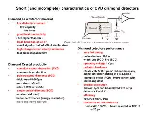
Introduction / Motivation NoRHDia – Novel Radiation Hard Diamond Detectors for Hadron Physics GSI, Darmstadt – Heavy Ions (HI) accelerator, p-U, up to several AGeV GOAL: Fast radiation hard diamond detector of spectroscopic properties for timing (start detector of ToF) of HI and ΔE spectroscopy of HI Why to develop particle detectors using new materials ? future (and some present) HP experiments require detectors of high rate (1GHz/cm2) capability and radiation hardness (neq~1016 cm-2) - beyond standard silicon technology Why diamond ? large band gap – no cooling, no pn junction, high resistivity, solar-blind rigid lattice – high drift velocity saturation, high thermal conductivity high C binding energy – radiation hard Why novel and not new material ? IIa natural & HPHT diamond – atomic impurities limit charge transport (expensive, high selectivity, not reproducible) pcCVD diamond – grain boundaries limit charge transport (still good for some applications) scCVD detector development triggered by: Isberg et al., Science, 2002 electronic grade of extraordinary mobility and lifetime 1/11 Michal Pomorski – GDR, 13-15 October, Supelec, Gif-sur-Yvette
2. Electronic properties(EP) - dark current - charge transport - α-particles spectroscopy • Material quality • - atomic impurities • - structural defects collected charge induced current i(t) Q(t) integration 3. Radiation tolerance - EP after high fluence ir. t t • 4. In-beam perform. • - HI timing • - HI ΔE spectroscopy Useful parameters: CCE = Qcoll/Qgen Qcoll= Qgen·τeff/ttr·(1-exp(-ttr/τeff)) CCD = 1/e * Qgen • Induced signal defined by: • device geometry • generated charge • internal E • drift velocity(E) / mobility • lifetime Solid-state particle detector basics and OUTLINE Qgen ~ ΔE/εavg 2/11 Michal Pomorski – GDR, 13-15 October, Supelec, Gif-sur-Yvette
5 mm Michal Pomorski – GDR, 13-15 October, Supelec, Gif-sur-Yvette 1. Material: atomic,macroscopic defects • Free-standing <100> homoepi. scCVD • by Element 6 • □ 5x5 mm2 50-500 μm • Atomic impurities (most common in CVD): • nitrogen (P1 center) < 1014 cm-3 • (below ESR detection limit) • boron acceptors ~ 1015 cm-3 (TPYS) • Microscopic structural defects: • threading dislocations + extended defects • high strain • good quality also possible (recent samples) white beam X-ray diffraction topography, ESRF Birefringenceimaging using VIS and crosspolar. M.P. Gaukroger et al., Diam Relat. Mat. 2008 3/11
Michal Pomorski – GDR, 13-15 October, Supelec, Gif-sur-Yvette 2. Electronic Properties: dark current-I-V characteristics ◊ dark current correlated with structural defects ◊ SCL charge injection electroluminescence ◊ defect-free scCVD: E >10 V/μm with I < 1pA 4/11
Michal Pomorski – GDR, 13-15 October, Supelec, Gif-sur-Yvette 2. Electronic Properties: charge transport by TCT (ToF) induced (transient) currents in 300 μm scCVD data points ~15 samples vdr=d/ttr E(x) = const. (no space charge) no visible decay of drifting charge: τeff[ns]: e ~200-400, h ~200-1000 Life time >> drift time (~few ns) μ0 [cm2/Vs]: e ~4500, h ~2800 (4x Si) Directly measured μeff(E): e 1800@0.1V/μm, h 2400@0.06V/μm vsat [x107 cm/s]: e ~2.6, h ~1.6 (4xSi) Directly measured v(E) @ 10V/μm: e 1.4, h 1.4 CCD order of several cm ! 5/11
Michal Pomorski – GDR, 13-15 October, Supelec, Gif-sur-Yvette 2. Electronic Properties: α-spectroscopy - approaching silicon detectors 241Am α-source spectra ·5.5 MeV • ◊ ΔE/E~0,3 % common (>30 scCVD) spectroscopic properties • ◊ saturation of charge collection at low E < 0.3 V/μm • ◊ stable operation, no polarization effect 6/11
Michal Pomorski – GDR, 13-15 October, Supelec, Gif-sur-Yvette 3. Radiation Tolerance: radiation inducedeffects 26 MeV p ~20 MeV n 26 MeV protons 6x more damaging than ~20 MeV neutrons ≤ 1.6 x 10¹⁶ p/cm2 NIEL ~ 130 MeVmb ≤ 2.1 x 10¹⁵ p/cm2 NIEL ~ 20 MeVmb 6.1 x 1014 cm-2 6.4 x 1013 cm-2 τ ~ 10 ns τ ~ 1 ns ◊ dark current drops, RT operation possible, noise not changed ◊ drift velocity not changed, no space charge (neutral defects - mainly V0) ◊ linear drop of τeff with fluence, similar for p an n 7/11
Michal Pomorski – GDR, 13-15 October, Supelec, Gif-sur-Yvette 3. Radiation Tolerance: CCD vs. fluence RD42 S/N~15 limited by electronics ◊ ~2.3 increase in CCD due to priming effect (Lazarus at RT) ◊ after ~1016 26 MeV p/cm2 still good S/N ◊ most pessimistic scenario can be improved by annealing (studied), device engineering... 8/11
Michal Pomorski – GDR, 13-15 October, Supelec, Gif-sur-Yvette 4. In-beam Performance: HI timing, ΔE spectroscopy @ GSI HI timing HI ΔE spectroscopy @ FRS 132Xe fragmentation D2:STOP D1:START Z=48... Z=47 Z=46 ...Z=45 ΔE/E ~1% • a large (50m) mass spectrometer @ GeV • 103 higher ΔE than α-particles SCL regime • excelent stability and ΔE/E ~ 1% (limited • by starggling not by detector) 9/11
Michal Pomorski – GDR, 13-15 October, Supelec, Gif-sur-Yvette Summary • Material quality: • high purity material (atomic impurities) • structural defects threading dislocations • 2. Electronic properties: • structural defects limit dielectric strength and govern dark current behaviour • drift velocity (and mobility) limited only by intrinsic diamond properties • lifetime of charge carriers >> drift time huge CCD ~full CCE • scCVD diamond is a spectroscopic grade material (as good as Si) • 3. Radiation tolerance (26MeV p, and 20 MeV n irradiation) • drop of CCD,but no increase of leakage current • operation with good S/N after ~1x10¹⁶ p/cm2 still possible (at RT) • 4. Detector prototypes: • - timing; heavy ions σ < 30ps • - energy loss spectroscopy of heavy ions 10/11
Michal Pomorski – GDR, 13-15 October, Supelec, Gif-sur-Yvette Present/Future work @ CEA-Saclay • since ~ 2 months at LCD of CEA-Saclay... • Diamond Radiation Detectors Group: D. Tromson, Ch. Mer, M. Rębisz-Pomorska, P. Bergonzo • Finishing upgrade of the diamond detectors characterization station: • transient current technique (drift velocity, internal field prof.) • CCE and spectroscopy (homogeneity, lifetime) • CCD/CCE of low quality or damaged diamonds - 90Sr + triggering • Single Crystal Growth by CVD: • - electronic quality intrinsic scCVD • - intrinsic+boron doped - thin films α-particles/n detectors • also looking forward to test your samples..... • large area thicksingle crystal diamonds are specially welcome 11/11
~1 cm2 scCVD ESRF Grenoble, X-rays Some scCVD applications as particle detector HADES @ GSI Beam postion, intensity monitoring Thank you for your attention! CMS @ LHC start & veto detectors Hadron therapy @ GSI Beam condition monitoring ATLAS @ LHC JET, Chulam, UK First scCVD pixel detector VUV, UV spectroscopic monitoring Heavy ions counting
„raw” film detector prototype <100> cleaning and oxidation: hot acids electrodes sputtering: Al(100nm) Cr(50nm)Au(100nm) packaging: mounting, bonding, RF-design Michal Pomorski – GDR, 13-15 October, Supelec, Gif-sur-Yvette 2. Electronic Properties: detector fabrication and meas. techniques Detector fabrication • Dark (leakage) current • CCE / ΔE spectroscopy: • CS low noise electronics • CCE / CCD (damaged detectors): • traversing particles – e from 90Sr • CS electronics Transient Current Technique DSO/3GHz Diamond detector CD ~1pF BB amlifier/2GHz 4/12
Motivation • Requirements for solid-state particle Detectors in future hadron physics experiments (FAIR, sLHC): • high rate capabilities • rates ~ 3 x 109 cm-2s-1 • radiation hardness • intergral fluence ~ 1 x 10¹⁶ pcm-2 at the limit (or beyond) standard silicon technology... try to use other materials which may challenge Si in future detector development.... • one of the most promising: DIAMOND (scCVD): • large band gap, low capacitance, high resistivity, high thermal conductivity, high • drift velocity saturation, radiation hard scCVD detector development triggered by: Isberg et al., Science, 2002 GOAL: Fast radiation hard diamond detector of spectroscopic properties 1/13 Michal Pomorski – GDR, 13-15 October, Supelec, Gif-sur-Yvette
Michal Pomorski – PhD debate, Frankfurt University 07/08/2008 2. Electronic Properties: spatial mapping of charge transport - XBIC defective scCVD ~6keV X-rays Down to 1μm() beam spot X-ray beam time structure measured with scCVD defect-free scCVD • defective crystals: • charge trapping at dislocations (low E) • breakdown behaviour at dislocations (high E) • persistent current at surfaces defects • defect-free crystals: • perfect homogeneity of charge collection • perfect stability, rates ~1013 mip s-1·cm-2 8/13
Motivation GSI & FAIR HI accelerator • Requirements for solid-state particle • Detectors in future hadron physics • Experiments (FAIR, sLHC): • high rate capabilities • rates ~ 3 x 109 cm-2s-1 • radiation hardness • Intergral fluence ~ 1 x 1016cm2 5 cm from target: 3x109 cm-2s-1 Φ > 1x10¹⁵ neq /cm2/year at the limit (or beyond) standard silicon technology... Tasks of this PhD / outline of this talk try to use other materials which may challenge Si in future detector development.... • one of the most promising: DIAMOND (scCVD): • large band gap, low capacitance, high resistivity, high thermal conductivity, high • drift velocity saturation, radiation hard scCVD detector development triggered by: Isberg et al., Science, 2002 GOAL: Fast radiation hard diamond detector of spectroscopic properties 1/12 Michal Pomorski – GDR, 13-15 October, Supelec, Gif-sur-Yvette
Michal Pomorski – PhD debate, Frankfurt University 07/08/2008 4. In-beam Performance: HI spectroscopy @ FRS of GSI FRS GSI 132Xe – projectile and its fragments ◊ energy – 200AMeV – 1.2AGeV fragments@740AMeV 36<Z<54 deposited energy 0.5-1.6 GeV ◊ ΔE/E ~1.5-2% (limited by straggling) ◊ HI fragments identification possible ◊ SCL transport of charge carriers ◊ better performance than Si Transient currents: SCL transport 13/15
Michal Pomorski – PhD debate, Frankfurt University 07/08/2008 4. In-beam Performance: HI, MIPtiming @ GSI stop start Intrinsic resolution ◊ heavy ions σintr=28ps (electronic limitation) ◊ MIP (3.5 GeV p) σintr ~100ps (S/N limitation) ◊ detection efficiency HI ~98%, MIP~95% 12/15
silicon diamond Vacancy + Interstitial ED>40 eV V Particle + C I band structure trapping/re-trapping CB e e donor + - + acceptor - h h VB generation Radiation induced effects: ◊ in full energy range NIELDiam < NIELSi ◊ low energies: NIELDiam ~ 1/3 NIELSi ◊ high energies: NIELDiam ~ 1/10 NIELSi ◊ decrease of lifetime ◊ increase of leakage current ◊ generation of space charge Michal Pomorski – PhD debate, Frankfurt University 07/08/2008 3. An Insight into Radiation Tolerance: non-ionizing energy losses Is NIEL representative for the detector operation? 9/15
collected charge induced current „raw” film detector prototype i(t) Q(t) integration t t <100> cleaning and oxidation: hot acids electrodes sputtering: Al(100nm) Cr(50nm)Au(100nm) packaging: mounting, bonding, RF-design Detector fabrication Michal Pomorski – PhD debate, Frankfurt University 07/08/2008 Basics of Particle Detection: solid-state ionization chamber ionization drift-diffusion signal processing Ramo theorem: i(t)=-q·Ew·v Ideal case: ~100% charge collection, homogenous In practice: charge trapping, inhomogenous, break down Evaluation criteria: Idark, τeff –life time, vdr(E) – drift velocity CCD- charge collection distance, limited by: CCD=vsatτeff CCE= CCD/d (1-exp(-d/CCD)) 4/15
Michal Pomorski – PhD debate, Frankfurt University 07/08/2008 Why Diamond ?: some physical properties + no leakage, no pn, no cooling + faster charge collection + lower capacitance + more radiation hard -/+ lower signal 2/15
Michal Pomorski – PhD debate, Frankfurt University 07/08/2008 2. Electronic Properties: charge transport - transient current technique transient currents in scCVD V(E)=d/ttr if E(x)=const. data points ~15 samples ttr E(x) = const. (no space charge) μ0 [cm2/Vs]: e ~4500, h ~2800 Directly measured μeff(E): e 1800@0.1V/μm, h 2400@0.06V/μm vsat [x107 cm/s]: e ~2.6, h ~1.6 Directly measured v(E) @ 10V/μm: e 1.4, h 1.4 τeff[ns]: e ~200-400, h ~200-1000 Life time >> drift time speed of the detector limited by e drift in broad range of E CCD order of several cm ! 6/15
Michal Pomorski – PhD debate, Frankfurt University 07/08/2008 3. An Insight into Radiation Tolerance: radiation inducedeffects 26 MeV p ~20 MeV n 6.1 x 1014 cm-2 6.4 x 1013 cm-2 ≤ 1.6 x 10¹⁶ p/cm2 NIEL ~ 130 MeVmb ≤ 2.1 x 10¹⁵ p/cm2 NIEL ~ 20 MeVmb τ ~ 1 ns τ ~ 10 ns 1/τeff =β·Φ ◊ drift velocity not changed ◊ no space charge (neutral defects) ◊ linear drop of τeff with fluence ◊ τeff drop does not scale with NIEL 10/15
Michal Pomorski – PhD debate, Frankfurt University 07/08/2008 An Insight into Radiation Tolerance: charge collection Priming ! (Lazarus effect at RT) neutron irradiation; MIP (90Sr source); CSE 11/15
Michal Pomorski – PhD debate, Frankfurt University 07/08/2008 An Insight into Radiation Tolerance: radiation induced effects signal formation charge collection proton irradiation; 241Am α-source; BB neutron irradiation; 90Sr source; CSE proton irradiation; 90Sr source; CSE • lifetime reduction, no space charge • no additional scattering, velocity not changed • β~20MeVn = β26MeVp doesn’t scale with NIEL • βdiam>βSi (no re-trapping) • priming (pumping, Lazarus) effect @ RT • space charge polarization • CCE decreases with dose • σ/MPV not changed up to 1015 cm-2 11/15
Michal Pomorski – PhD debate, Frankfurt University 07/08/2008 An Insight into Radiation Tolerance: irradiations, defects 26 MeV p ~20 MeV n Defects identification by optical methods absorbtion Karlsruhe Louvain-la-Neuve Up to ~2x10¹⁵ p/cm2 Up to ~1x10¹⁶ p/cm2 Mainly GR1 Neutral mono-vacancy Weak R2,R11 Split-interstitial Residual complex (PL) NV0, others no di-vacancies, clusters others optically not active (?) photoluminescence dark current 10/15
I(t) induced current „raw” film detector prototype t Q(t) collected charge <100> t Cleaning and Oxidation: hot acids Electrodes sputtering: Al(100nm) Cr(50nm)Au(100nm) Packaging: mounting, bonding, RF-design Michal Pomorski – PhD defense 07/08/2008 Basics of Particle Detection: solid state ionization chamber IonizationDrift-diffusionSignal processing parallel plate geometry Ramo theorem i(t)=-q·Ew·v more complicated geometries num. simulations Importnat parameters for signal formation: Detector fabrication ve,h(E) = μe,h(E)·E(x) – velocity,mobility τeff – effective life time CCD- charge collection distance, averaged „Schubweg” for e and h ne,h =1/e Limited by: CCD=vsatτeff CCE – charge collection efficiency
Motivation CBM @ FAIR • New physics (QGP, Higgs) will be studied in • rare proceses • - increase in beam energy • increasy in beam intensity • leads to • high detector occupancy (fast detectors, large granurality) • radiation damage (radiation hard detectors) • At the limit (or beyond) standart silicon technology Si detectors: material engineering, device engineering and change of detector operational conditions 5 cm from target: Another idea is to study new materials for use in particle detection.....diamond, SiC, GaN... particle flow ~ 3x109 cm-2s-1 Φ > 1x10¹⁵ neq/cm2/year Novel Radiation Hard Diamond Detectors For Hadron Physics in frames of I3HP ATLAS @ (s)LHC most inner layer: Φ ~ 1.6 x 10¹⁶ neq/cm2/5 years • Deliverables: • radiation hard scCVD-DD prototype • for mip timing (σ<100ps) • heavy ions spectroscopy (ΔE/E~few %) L ~ 1035 cm-2s-1 Michal Pomorski – PhD debate, Frankfurt University 07/08/2008
Michal Pomorski – PhD defense 07/08/2008 Some History Not new but... Novel material Diamond material sc CVD of electronic qua. e6 first CVD synthesis NIRIM first HPHT synthesis sc heptx CVD age ? sc CVD age natural diamond age poly CVD age HPHT age 2004 2002 1981 1955 this work High selectivity - very rare only intrinsic diamond limitation??? high atomic contamination Diamond detectors grain boundaries
Motivation CBM @ FAIR ATLAS @ (s)LHC most inner layer: L ~ 1035 cm-2s-1 Φ ~ 1.6 x 10¹⁶ neq/cm2/5 years 5 cm from target: particle flow ~ 3x109 cm-2s-1 at the limit (or beyond) standard silicon technology... Φ > 1x10¹⁵ neq/cm2/year Novel Radiation Hard Diamond Detectors For Hadron Physics in frames of I3HP • Deliverables: • radiation hard scCVD-DD prototype • for mip timing (σ<100ps) • heavy ions spectroscopy (ΔE/E~few %) Michal Pomorski – PhD debate, Frankfurt University 07/08/2008
Many valleys semiconductor Different m* cold and hot valleys Heating and scattering Repopulation effect <100> most „cold” possibility for e <100> most „hot” possibility for h result vh> ve 0.3 – 11 V/μm
“kinematic term” “minimum ionizing particles” 3-4 “relativistic rise” density effect Bethe-Bloch Formula ionization constant
Michal Pomorski – PhD defense 07/08/2008 Some History Eversol, Angus, Deryagin 56-68, diamond CVD Spitsin et al. 81’ H in CVD Isberg et all. Diamond material sc CVD of electronic qua. e6 first CVD synthesis NIRIM first HPHT synthesis sc heptx CVD age ? sc CVD age natural diamond age poly CVD age HPHT age 2004 2002 1981 1955 this work High selectivity - very rare only intrinsic diamond limitation??? high atomic contamination 1663 – sir Boyle „glowing diamonds” first TL detectors Diamond detectors grain boundaries pcCVD HI detectors at GSI pcCVD RD42 at CERN
Electronic Properties: I-V characteristics,dark current Electroluminescence from defective crystal I-E(V) characteristics ~13 samples Presence of structural defects govern I-V characteristics and dielectic strenght
Michal Pomorski – PhD debate, Frankfurt University 07/08/2008 An Insight into Radiation Tolerance: non-ionizing energy losses Mika Huhtinen NIMA 491(2002) 194 silicon diamond 10 MeV n 10MeV p W. de Boer et al.arXiv:0705.0171v1 24 GeV p band structure V0 in diamond trapping/re-trapping CB e e donor + - + acceptor - h In whole energy range NIELDiam < NIELSi h VB generation Radiation induced defects decreases life time of charge carriers: ◊ at low energies: NIELDiam ~ 1/3 NIELSi ◊ at high energies: NIELDiam ~ 1/10 NIELSi Is NIEL representative for the detector operation? what about defects evolution after irrad., trapping -re-trapping etc. (?) Other effects (more important in Si): ◊ increase of leakage current ◊ generation of space charge 9/15
Michal Pomorski – PhD debate, Frankfurt University 07/08/2008 Electronic Properties: response to ionizing radiation 241Am α-source 90Sr β-source; ~MIP charge collection charge collection εavg=12.86 eV/e-h • ΔE/E~0,3 % common spectroscopic properties (first time in DD development) • - saturation of charge collection at low E < 0.3 V/μm – almost complete charge collection • MIP distribution – narrower widths, higher cut-off at low energy than in Si 7/14
Motivation / Tasks of the Thesis Michal Pomorski – PhD debate, Frankfurt University 07/08/2008 CBM @ FAIR another approach to this problem... try to use other materials which may challenge Si .... one of the most promising: DIAMOND (scCVD) scCVD detector development triggerd by: Isberg et al., Science, 2002 material quality electronic properties 5 cm from target: particle flow ~ 3x109 cm-2s-1 radiation tolerance Φ > 1x10¹⁵ neq /cm2/year in-beam operation – detector prototypes at the limit (or beyond) standard silicon technology... Novel Radiation Hard Diamond Detectors For Hadron Physics in frames of I3HP New development in Si tech.: • Deliverables: • radiation hard scCVD-DD prototype • for MIP timing (σ<100ps) • heavy ions spectroscopy (ΔE/E~few %) material engeenering devices engineering cooling etc. 1/15
Michal Pomorski – PhD debate, Frankfurt University 07/08/2008 Why Diamond ?: some physical properties crystal structure: FCC a=0.15 nm (most „packed” solid) simplified band structure detector operation: • + no leakage current (no junction, no cooling) • + faster charge collection • + lower capacitance • + more radiation hard • + lower background • - lower generated signal 2/15
Motivation / Tasks of the PhD Michal Pomorski – PhD debate, Frankfurt University 07/08/2008 CBM @ FAIR another approach to this problem... try to use other materials which may challenge Si .... one of the most promising: DIAMOND (scCVD) scCVD detector development triggered by: Isberg et al., Science, 2002 Novel material of unknown properties 5 cm from target: Tasks of this PhD / outline of this talk particle flow ~ 3x109 cm-2s-1 material quality Φ > 1x10¹⁵ neq /cm2/year electronic properties at the limit (or beyond) standard silicon technology... radiation tolerance in-beam operation – detector prototypes 1/15