Download
1 / 69
870 likes | 1.42k Views
Fluorescence Spectroscopy. Source. CHM 5175: Part 2.5. Detector. h n. Sample. Ken Hanson MWF 9:00 – 9:50 am Office Hours MWF 10:00-11:00. Fluorescence Spectroscopy. Filter Church Window 400nm SP filter. First observed from quinine by Sir J. F. W. Herschel in 1845.

E N D
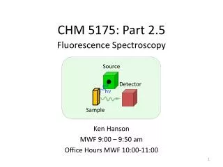
Fluorescence Spectroscopy Source CHM 5175: Part 2.5 Detector hn Sample Ken Hanson MWF 9:00 – 9:50 am • Office Hours MWF 10:00-11:00
Fluorescence Spectroscopy Filter Church Window 400nm SP filter • First observed from quinine by Sir J. F. W. Herschel in 1845 Yellow glass of wine 400 nm LP filter hn Quinine Solution (tonic water) Observe Blue emission Herschel concluded that “a species in the solution exert its peculiar power on the incident light and disperses the blue light.”
Fluorescence Spectroscopy Measuring the light given off by an electronically excited state. Ground State (S0) Singlet Excited State (S1) hn Fluorescence hn Excitation Emission Intersystem Crossing hn Phosphorescence Emission Triplet Excited State (T1)
Fluorescence Spectroscopy Singlet Excited State (S1) Fluorescence Spin allowed Fast (ns) Organic molecules hn Emission Triplet Excited State (T1) Phosphorescence Spin “forbidden” slow (ms to s) Transition metal complexes hn Emission
Jablonski Diagram S2 Excitation Internal Conversion Fluorescence Non-radiative decay Intersystem Crossing Phosphorescence S1 T2 Energy T1 S0
Fluorescence S2 • 1) Excitation • -Very fast (< 10-15 s) • -No structure change • 2) Internal Conversion • -Fast (10-12 s) • -Structure change • 3) Fluorescence • -”Slow” (10-9 s) • - No structure change 2 1 S1 Energy 3 S0 Geometry
Fluorescence Snail (0.005 m/s) Sprinter (7 m/s) n3 S2 n2 n1 IC n3 S1 n2 n1 Internal Conversion (sprinter) “always” wins! Absorption Fluorescence Kasha’s Rule: Emission predominantly occurs from the lowest excited state (S0 OR T1) S0 • Internal Conversion (1012 s-1) • S2 Fluorescence (109 s-1)
Fluorescence Kasha Laboratory Building AKA Institute of Molecular Biophysics 1920-2013 Kasha’s Rule: Emission predominantly occurs from the lowest excited state (S0 OR T1)
Fluorescence Kasha’s Rule: Emission predominantly occurs from the lowest excited state (S0 OR T1) Red Lower E Blue Higher E S1 S0 Internal Conversion Eabsorption > Eemission Emission is red-shifted (bathochromic) relative to absorption Absorption is blue-shifted (hypsochromic) relative to emission
Mirror Image Rule • Vibrationallevels in the excited states and ground states are similar • An absorption spectrum reflects the vibrational levels of the electronically excited state • An emission spectrum reflects the vibrational levels of the electronic ground state • Fluorescence emission spectrum is mirror image of absorption spectrum v’=5 v’=4 v’=3 v’=2 v’=1 S1 v’=0 v=5 v=4 v=3 v=2 v=1 S0 v=0
Mirror Image Rule n4 n3 S1 n2 n1 n4 n3 n2 S0 n1
Mirror Image Rule fluorescein ethidium bromide Anthracene
Stokes Shift Stokes Shift: Difference in energy/wavelength between absorption max and emission max. S1 S0 Internal Conversion Sensitivity to local environment: Solvent polarity Temperature Hydrogen bonding
Solvent Dependence Stokes Shift: Difference in energy/wavelength between absorption max and emission max. 4-dimethylamino-4'-nitrostilbene (DNS) Solvatochromism
Jablonski Diagram S2 Excitation Internal Conversion Fluorescence Non-radiative decay Intersystem Crossing Phosphorescence S1 T2 Energy T1 S0 hn Intersystem Crossing Emission Ground State (S0) Singlet Excited State (S1) Triplet Excited State (T1)
Phosphorescence S2 • 1) Excitation • -Very fast (10-15 s) • -No structure change • 2) Internal Conversion • -Fast (10-12 s) • -Structure change • 3) Intersystem Crossing • -Fast (10-12 s) • -No Structure change • 4) Phosphorescence • -”Slow” (10-6 s) • - No structure change T2 2 3 S1 2 1 T1 E 4 2 S0 Geometry
Emission Fluorescence Phosphorescence Slow (10-6 – 0.1 s-1)>microseonds >100 nm Yes Rates: Lifetime: Dl: O2 sensitive: Fast (10-9s-1)nanoseconds <100 nm no
Fluorescence vs Phosphorescence Internal Conversion (10-12 s) S2 Intersystem Crossing w/ Heavy atom (< 10-12 s) w/o Heavy atom (> 10-9 s) S1 E T1 Excitation (10-15 s) Fluorescence (10-9 s) Phosphorescence (10-6 s) S0
Emissive Molecules Phosphorescent Fluorescent PtOEP Ir(ppy)3 OEP Perylene [Ru(bpy)3]2+ Rose Bengal BODIPY Fluorescein Anthracene + ICH3 Coumarin C60 Anthracene
Fluorometer Source Excitation hn Detector Sample hn Emission Variables Excitation Wavelength Excitation Intensity Emission Wavelength Filters
Fluorometer 3 1 2 Components 1) Light source 2) Monochrometer 3) Sample 4) Detector 5) Filters 6) Slits 7) Polarizers 4 2
Fluorometer: Simple Diagram Xenon Lamp Grating Mirrors Excitation Monochromator Emission Monochromator PMT Two light sources = Two monochromators! 1 for excitation 1 for emission Sample Grating
Fluorometer: Medium Diagram Grating Mirror Mirror Lens Sample
Fluorometer: Hard Mode Grating Mirrors Mirror Grating
Fluorometer: Hard Mode 2 450 W Xe 300 nm blaze 1200 g/mm exit slit iris NIR: 9170-75=950-1700 nm 1000 nm blaze 600 g/mm grating shutter polarizer slit r UV-VIS: R928 = 250-850nm 500 nm blaze 1200 g/mm grating V V V
Horiba JY Fluoromax-4 Horiba JY Fluoromax-4 MAC Lab (Materials Characterization) Dr. Bert van de Burgt CSL 116
Measuring Emission Spectra Xenon Lamp Procedure 1) White light source on 2) Shift excitation grating to desired wavelength (excitation wavelength) 3) Light enters sample chamber 4) Light Hits the Sample 5) Emission from the sample enters emission monochromator 6) Set emission grating 7) Detect emitted light at PMT 8) Raster emission grating Excitation Monochromator 1 Ex Grating Emission Monochromator 2 3 PMT 7 5 4 6 8 Sample Em Grating
Measuring Emission Spectra Absorption Spectrum Procedure 1) White light source on 2) Shift excitation grating to desired wavelength (excitation wavelength) 3) Light enters sample chamber 4) Light Hits the Sample 5) Emission from the sample enters emission monochromator 6) Set emission grating 7) Detect emitted light at PMT 8) Raster emission grating Emission Spectrum Excitation at 450 nm Emission from 550 – 900 nm
Excitation Spectrum n3 S3 n2 n1 S3 n3 S2 n2 n1 IC n3 S1 n2 S1 S2 n1 Absorption Fluorescence Fluorescence emission spectrum is the same regardless of the excitation wavelength! S0
Excitation Spectrum n3 S3 n2 n1 n3 S2 n2 n1 IC Absorbance n3 S1 n2 n1 Fluorescence emission spectrum is the same regardless of the excitation wavelength! Absorption Fluorescence But intensity changes! S0
Excitation Spectrum Monitor emission (Fixed l) Absorbance Scan Through Excitation l
Measuring Excitation Spectra Xenon Lamp Procedure 1) Shift emission grating to desired wavelength (monitor emission max) 2) Shift excitation grating to stating wavelength 3) Light source on 4) Light Hits the Sample 5) Emission from the sample enters emission monochromator 6) Detect emitted light at PMT 7) Raster excitation grating Excitation Monochromator 3 Ex Grating Emission Monochromator 2 7 PMT 6 5 4 1 Sample Em Grating
Excitation Spectrum Absorption Spectrum Excitation Spectrum If emitting from a single species: Excitation spectrum should match absorption spectrum!
Fluorometer 3 1 2 Components 1) Light source 2) Monochrometer 3) Sample 4) Detector 5) Filters 6) Slits 7) Polarizers 4 2
Samples Solutions Thin Films Crystals Powders
Solution Fluorescence Top View Source Excitation Beam Emission Excitation hn Detector Sample hn Emission non-emitting molecules filter effect “self”-absorption
Filter Effect Anthracene For Fluorescent Samples: Absorbance < 1.0
Solid Samples Emission Spectrum Thin Films/Solids Ex: 380 nm Source Detector Sample Real emission spectrum + Second Order
Solid Samples Emission Spectrum Thin Films/Solids Ex: 380 nm Source Detector 2d λ = 2d(sin θi + sin θr) Sample Detector at 760 nm sees 380 nm light! Real emission spectrum + Second Order
Filters Band Pass Filter
Fluorometer 3 1 2 Components 1) Light source 2) Monochrometer 3) Sample 4) Detector 5) Filters 6) Slits 7) Polarizers 4 2
Fluorometer: Slits Entrance Slit Mirrors Exit Slit
Slit widths Entrance Slit Wider Slits: More light hitting sample More emission More light hitting the detector More signal Greater signal-to-noise But…resolution decreases! Exit Slit Entrance Slit Source hn Sample
Slit widths Entrance Slit Source hn Sample Small Slit Large Slit bandpass (nm) = slit width (mm) x dispersion (nm mm-1) for a 4.25 nm mm-1 grating
Excitation Slit widths Single Component: Wider slit: Larger bandwidth Intensity increase No emission spectra change Absorbance
Excitation Slit widths Multi Component : Wider slit: Larger bandwidth Intensity increase Emission ratio changes (1:2) -small slit less of dye 2 -large slits more of dye 2
Emission Slit widths Wider slit: Larger bandwidth More light hitting the detector More signal Lower Resolution Exit Slit hn Grating Detector Sample doubled slits = intensity2 570 nm emission Large Slit (2.0 mm) Small Slit (0.5 mm) summing 566-574 nm (8.5 nm bandwidth) summing 569-571 nm (2.125 nm bandwidth) Nyquist Rule: scanning increment should be greater than 1/2 slit widths Ex: For 8 nm bandwidth set emission acquisition to 4 nm per step.