Download
1 / 29
290 likes | 293 Views
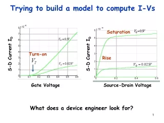
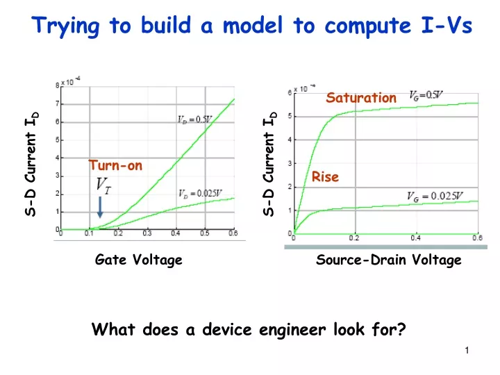
Trying to build a model to compute I-Vs. Saturation. S-D Current I D. S-D Current I D. Turn-on. Rise. Gate Voltage. Source-Drain Voltage. What does a device engineer look for?. Top-down vs. Bottom-up. L > 1 m m. L ~ 100s nm. L ~ 10 nm. drain. source. Ballistic QM “ Nano ”

E N D
Trying to build a model to compute I-Vs Saturation S-D Current ID S-D Current ID Turn-on Rise Gate Voltage Source-Drain Voltage What does a device engineer look for?
Top-down vs. Bottom-up L > 1 mm L ~ 100s nm L ~ 10 nm drain source Ballistic QM “Nano” Critical role of Contacts Quantum Dynamics in Channel + Stat Mech in Contacts Semiclassical Transport/ “Meso”scopics Critical Role of Quantum Mechanics Drift-Diffusion (“Macro/Micro”) Classical Mechanics + Statistical Mechanics Mixed up
Small is different ! Ohm’s Law Where is the Transition? R = rL/A R = h/2q2 ~ 13 KW = h/2q2[(1 + L/l)/M] R = r(L + l)/A M: # of modes, l : mean-free-path
What is resistance? R not a simple sum of R1 and R2 !
Starting point: Band-diagram Solids have energy bands (Ch 5)
Empty levels Filled levels Semiconductor (Si) (charge movement can be controlled) Metal (Copper) (charges move) Insulator (Silica) (charges can’t move) Filling up the Bands with Electrons E
Fermi Energy (electro- chemical potential) EF Drain Source Separating filled and empty levels conduction band valence band
E Empty kBT Filled f0(E-EF) f0(E-EF) 0 1 f0(E) =1/(eE/kBT + 1) Drain Source Average occupancy (Fermi function) EF Boltzmann Constant: kB = 1.38 x 10⁻²³ JK-1 Room Temperature T=300K, Thermal Energy kBT = 4.14 x 10⁻²¹ J (To get eV, divide by q=1.6 x 10⁻¹⁹C), so Room temperature ~ 25 meV
Role of Gate Create levels at Fermi Energy VG = 0 VG > 0 n type operation Vacuum Level Vacuum Level • Fermi energy held fixed by source and drain • Conduction depends on availability of states at EF
More electrons In plain English… VG > 0 n type operation Vacuum Level • Positive gate bias attracts electrons into channel • Channel now becomes more conductive
Fewer electrons p type operation VG < 0 Negative gate repels electrons and draws holes which conduct Vacuum Level Sufficient to have states at EF (filled or empty!) Two electrons per level (up and down spins)
Current onsets controlled by gate + Negative onset (EF to VB) Positive onset (EF to CB) SOURCE DRAIN CHANNEL INSULATOR Energy bands VG VD I (VD small, fixed)
From solid to molecule ID VG LUMO 0 V- V+ HOMO Current rises when level encountered Current falls when level crossed Gate scans states of the channel Discrete levels (smaller the molecule, more the separation)
How else could we bring levels near EF? Workfunction engineering (choose a contact material whose EF naturally lies near VB or CB) Vacuum level Low work function Cathode (eg. Ca) Molecular Layer High work function Anode (eg. ITO) Organic LEDs or OLEDS (not shown at equilibrium since EFs aren’t aligned)
How else could we bring levels near EF? Workfunction engineering (choose a contact material whose EF naturally lies near VB or CB) hn
qVD SOURCE DRAIN CHANNEL INSULATOR VG VD I What drives current? µ1 µ2 VD splits Fermi levels in source and drain Non-equilibrium Levels in the window sense a ‘difference of opinion’ between two contacts, and conduct as a result
Current flows due to difference in ‘agenda’ E E µ1 µ2 f1 f2 Only levels near EF conduct Need to complete loop to restore lost/gained charges
p vs n-type conduction µ1 µ1 µ2 µ2 Go thro’ level that is full at equilibrium (first eject charge then inject) Go thro’ level that is empty at equilibrium (first inject charge then eject) Battery removes the extra electron and hole in the contacts
Large Small Electrons spread out over molecule Electron sitting away from ends Escape time E E µ1 µ2 f1 f2 g: strength of bonding between contact and channel electrons g/ћ: inverse escape time into leads ћ = h/2p = 1.06 x 10⁻³⁴ Js g1 = 1 meV g1/ћ ≈ 1012/s = 1 THz
Toy Model : Current E E µ1 µ2 f1 f2 (weighted average of f1,2) (Only levels near EF conduct) (Net escape time 1/g = 1/g1 + 1/g2)
E E µ1 µ2 f1 Height 1/4kBT f2 Width kBT (-df0/dE)(m2-m1) (-df0/dE)qVD Finite temperature What does df0/dE look like?
E E µ1 µ2 f1 f2 1 - 0 MaximumConductance ?
E E µ1 µ2 f1 f2 MaximumConductance ? Conductance seems unlimited Experiment and calculation say otherwise !
G0 = 2q2/h = 77 mA/V Conductance quantization in gold nanowires EXPT Halbritter PRB ’04 Minimum resistance of a conductor (h/2q2 = 12.9 kW) Different from Ohm’s Law R = rL/A Modified Ohm’s Law R = r(L + L0)/A
Conductance quantization in gold nanowires EXPT Halbritter PRB ’04 G0 = 2q2/h = 77 mA/V Ohmic IV, quantized slope, fundamental constantsHow would this come from our equations?
E E µ1 µ2 f1 f2 For g1=g2, max conductance Solution: Broadening limits conductance “Spillage” Only fraction of level lies in m1-m2 window
Why do levels broaden? Fourier Transform P(t) D(E) t E Occupation probability Isolated channel Density of states (Sharp level) E=hn for quantum particles like electrons, photons Thus (t,E) form Fourier pairs
Why do levels broaden? e-t/t Fourier Transform e D(E) P(t) t E Occupation probability Channel coupled to contacts Density of states (Broadened level) D(E) = g/2p[(E-e)2 + (g/2)2] g = g1 + g2 = ħ/2t • Fourier transform of an exponent Lorentzian • peak value 2/pg, width ~ g • ∫D(E)dE = 1 (Sum rule Can still hold 1 electron)
µ1 µ2 T(E) Current with Broadening Landauer theory (“Conduction is Transmission”)