Download
1 / 23
240 likes | 555 Views
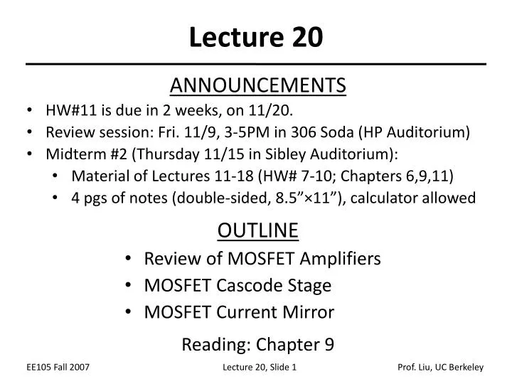
Lecture 20. ANNOUNCEMENTS HW#11 is due in 2 weeks, on 11/20. Review session: Fri. 11/9, 3-5PM in 306 Soda (HP Auditorium) Midterm #2 (Thursday 11/15 in Sibley Auditorium): Material of Lectures 11-18 (HW# 7-10; Chapters 6,9,11) 4 pgs of notes (double-sided, 8.5”×11”), calculator allowed.

E N D
Lecture 20 ANNOUNCEMENTS • HW#11 is due in 2 weeks, on 11/20. • Review session: Fri. 11/9, 3-5PM in 306 Soda (HP Auditorium) • Midterm #2 (Thursday 11/15 in Sibley Auditorium): • Material of Lectures 11-18 (HW# 7-10; Chapters 6,9,11) • 4 pgs of notes (double-sided, 8.5”×11”), calculator allowed OUTLINE • Review of MOSFET Amplifiers • MOSFET Cascode Stage • MOSFET Current Mirror Reading: Chapter 9
Review: MOSFET Amplifier Design • A MOSFET amplifier circuit should be designed to • ensure that the MOSFET operates in the saturation region, • allow the desired level of DC current to flow, and • couple to a small-signal input source and to an output “load”. • Proper “DC biasing” is required! (DC analysis using large-signal MOSFET model) • Key amplifier parameters: (AC analysis using small-signal MOSFET model) • Voltage gain Av vout/vin • Input resistance Rin resistance seen between the input node and ground (with output terminal floating) • Output resistance Rout resistance seen between the output node and ground (with input terminal grounded)
MOSFET Models • The large-signal model is used to determine the DC operating point (VGS, VDS, ID) of the MOSFET. • The small-signal model is used to determine how the output responds to an input signal.
Comparison of Amplifier Topologies Common Source • Large Av < 0 - degraded by RS • Large Rin • determined by biasing circuitry • Rout RD • ro decreases Av & Rout but impedance seen looking into the drain can be “boosted” by source degeneration Common Gate • Large Av > 0 -degraded by RS • Small Rin • - decreased by RS • Rout RD • ro decreases Av & Rout • but impedance seen • looking into the drain • can be “boosted” by • source degeneration Source Follower • 0 < Av ≤ 1 • Large Rin • determined by biasing circuitry • Small Rout • - decreased by RS • ro decreases Av & Rout
CS Stage Example 1 • M1 is the amplifying device; M2 and M3 serve as the load. Equivalent circuit for small-signal analysis, showing resistances connected to the drain
CS Stage Example 2 • M1 is the amplifying device; M3 serves as a source (degeneration) resistance; M2 serves as the load. Equivalent circuit for small-signal analysis
CS Stage vs. CG Stage • With the input signal applied at different locations, these circuits behave differently, although they are identical in other aspects. Common gate amplifier Common source amplifier
Composite Stage Example 1 • By replacing M1 and the current source with a Thevenin equivalent circuit, and recognizing the right side as a CG stage, the voltage gain can be easily obtained.
Composite Stage Example 2 • This example shows that by probing different nodes in a circuit, different output signals can be obtained. • Vout1 is a result of M1 acting as a source follower, whereas Vout2 is a result of M1 acting as a CS stage with degeneration.
NMOS Cascode Stage • Unlike a BJT cascode, the output impedance is not limited by .
Short-Circuit Transconductance • The short-circuit transconductance is a measure of the strength of a circuit in converting an input voltage signal into an output current signal: • The voltage gain of a linear circuit is (Rout is the output resistance of the circuit)
PMOS Cascode Current Source as Load • A large load impedance can be achieved by using a PMOS cascode current source.
MOS Current Mirror • The motivation behind a current mirror is to duplicate a (scaled version of the) “golden current” to other locations. Current Mirror Circuitry Current mirror concept Generation of required VGS
MOS Current Mirror – NOT! • This is not a current mirror, because the relationship between VX and IREF is not clearly defined. • The only way to clearly define VX with IREF is to use a diode-connected MOS since it provides square-law I-V relationship.
Example: Current Scaling • MOS current mirrors can be used to scale IREF up or down • I1 = 0.2mA; I2 = 0.5mA