Download
1 / 23
240 likes | 327 Views
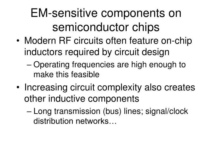
EM-sensitive components on semiconductor chips. Modern RF circuits often feature on-chip inductors required by circuit design Operating frequencies are high enough to make this feasible Increasing circuit complexity also creates other inductive components

E N D
EM-sensitive components on semiconductor chips • Modern RF circuits often feature on-chip inductors required by circuit design • Operating frequencies are high enough to make this feasible • Increasing circuit complexity also creates other inductive components • Long transmission (bus) lines; signal/clock distribution networks…
Motivation for modeling • Investigating parasitic effects • Vulnerability to external EM interference • Potential to create on-chip interference • Radiation • Substrate current • System-on-a-chip RF circuits require on-chip inductors with high L, small area and high Q • Automated design and speedy evaluation of geometrical tradeoffs.
Issues in modeling • Semiconductor substrates are conductive unable to treat system as metal/dielectric/ground plane • New processes feature higher doping, higher conductivity • Device circuits underneath metal structures display variable doping • Non-uniform substrate: n+ and p+ active regions, n-wells, p-wells, lightly doped chip substrate…
Inductor modeling---theory Modeling Approach:Divide a spiral inductor into segments and treat each current segment separately. Lkk=self-inductance (external+internal) of segment k Sources: Frequency-dependent current distribution within the segment and the magnetic flux linkage to the loop formed by the segment and its return current. Lkl=mutual inductance between segments k and l Sources: Magnetic flux linkage of the current in the first segment to the loop formed by the second segment and its return current. Lossy substrate effect: The return current has an effective distance into the substrate; this is frequency-dependent and can be modeled as a complex distance to account for the losses. Other frequency dependency: Skin effect in the metal; current crowding in the metal
Skin depth of semiconductor substrate Within our frequency range the skin depth will fall below our substrate thickness (around 5 GHz for p-type sub., around 2 GHz for n-well, lower for active regions)
External self-inductance Weisshaar et.al. showed in 2002 that an image current with a complex distance can be defined for the metal-oxide-lossy substrate system. ; Effective virtual ground plane distance from the signal current
Mutual inductance Mutual inductance: The magnetic flux created by the current on one loop linking to the area of other loop Calculate Y from the magnetic vector potential and I from the current distribution; the mutual inductance between two current segments is then Frequency dependency: The signal current of a current segment and its image current both induce voltages on the “target” current segment; the distribution of the image current varies with frequency on a semiconductor substrate.
Inductor modeling---Design issues • Variations in layout: • Metal layer • Length • Number of turns • Metal trace width • Metal trace spacing • Substrate doping • Shape • …
Some Results Substrate Doping Variation Overall, higher doping reduces inductance (closer return current, smaller loops) and makes it more freq-dependent (low enough doping pushes all current to bottom). Relationship between resistance and doping is not straightforward, since conductivity of substrate affects return current distribution, composition, and its frequency dependence all at the same time and these effects interact.
Inductors--- Test Chips • Designed for RF-probe station measurements • Manufactured through MOSIS • AMIS 0.5 μm; 3 Metal layers • Structures on chip 1: • Planar inductor on grounded poly • Planar inductor on n-well • Planar inductor on p-substrate • Planar inductor on n-plus • De-embedding structure: Open 4 5 1 2 3
Inductors--- Test Chips • Designed for RF-probe station measurements • Manufactured through MOSIS • AMIS 0.5 μm; 3 Metal layers • Structures on chip 1: • Planar inductor on pin-diode • Stacked inductor on p-substrate • Planar inductor on p-plus • De-embedding structure: Thru 3 4 2 1
De-embedding Open Thru DUT_full
De-embedding DUT_full: SDF ZDF, YDF Open: SOZO, YO Thru: STZT, YT ----DUT---- -----Ref. frame after Open is taken out------- --------Measured reference frame for DUT_full------------
De-embedding DUT_full: SDF ZDF, YDF Open: SOZO, YO Thru: STZT, YT YDF-O=YDF-YO YT-O=YT-YO ZDF-O ZT-O ZDUT=ZDF-O-ZT-O YDUT, SDUT