Download
1 / 1
10 likes | 195 Views
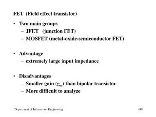
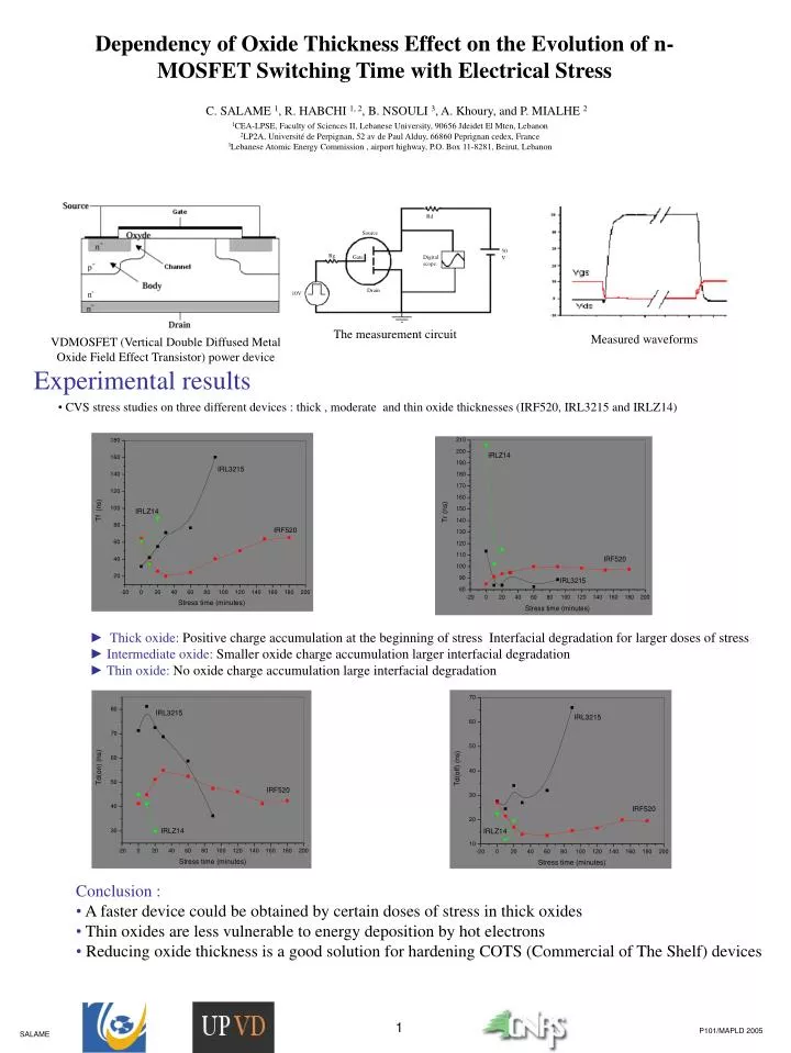
Rd. Source. 50V. Rg. Gate. Digital scope. Drain. 10V. The measurement circuit. Dependency of Oxide Thickness Effect on the Evolution of n-MOSFET Switching Time with Electrical Stress. C. SALAME 1 , R. HABCHI 1, 2 , B. NSOULI 3 , A. Khoury, and P. MIALHE 2.

E N D
Rd Source 50V Rg Gate Digital scope Drain 10V The measurement circuit Dependency of Oxide Thickness Effect on the Evolution of n-MOSFET Switching Time with Electrical Stress C. SALAME 1, R. HABCHI 1, 2, B. NSOULI 3, A. Khoury, and P. MIALHE 2 1CEA-LPSE, Faculty of Sciences II, Lebanese University, 90656 Jdeidet El Mten, Lebanon 2LP2A, Université de Perpignan, 52 av de Paul Alduy, 66860 Peprignan cedex, France 3Lebanese Atomic Energy Commission , airport highway, P.O. Box 11-8281, Beirut, Lebanon Measured waveforms VDMOSFET (Vertical Double Diffused Metal Oxide Field Effect Transistor) power device Experimental results • CVS stress studies on three different devices : thick , moderate and thin oxide thicknesses (IRF520, IRL3215 and IRLZ14) ► Thick oxide: Positive charge accumulation at the beginning of stress Interfacial degradation for larger doses of stress ► Intermediate oxide: Smaller oxide charge accumulation larger interfacial degradation ► Thin oxide: No oxide charge accumulation large interfacial degradation • Conclusion : • A faster device could be obtained by certain doses of stress in thick oxides • Thin oxides are less vulnerable to energy deposition by hot electrons • Reducing oxide thickness is a good solution for hardening COTS (Commercial of The Shelf) devices 1 P101/MAPLD 2005 SALAME