Download
1 / 32
390 likes | 758 Views
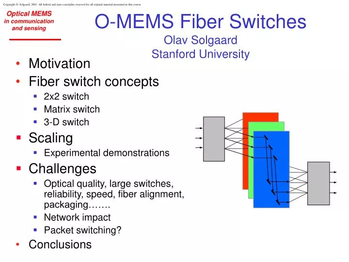
O-MEMS Fiber Switches Olav Solgaard Stanford University. Motivation Fiber switch concepts 2x2 switch Matrix switch 3-D switch Scaling Experimental demonstrations Challenges Optical quality, large switches, reliability, speed, fiber alignment, packaging……. Network impact

E N D
O-MEMS Fiber SwitchesOlav SolgaardStanford University • Motivation • Fiber switch concepts • 2x2 switch • Matrix switch • 3-D switch • Scaling • Experimental demonstrations • Challenges • Optical quality, large switches, reliability, speed, fiber alignment, packaging……. • Network impact • Packet switching? • Conclusions
Beam Steering Optical Switch • Analog mirrors • 2N scaling • Lucent, C-speed, Xros(NT),.....
Fresnel Zone Lens Fresnel Zone plate on polysilicon plate, which is rotated out of the plane on microhinges. The fact that the lens is an amplitude grating limits its diffraction efficiency. Lin, Lee, Pister, Wu, UCLA, 1994.
2 x 2 fiber-optic switch • Compact design • One-mask fabrication using DRIE on SOI • Integration of fibers, lenses, and micromirrors • 2 by 1 operation • By-pass switch • AT&T, JDSU....... Out 2 Out 1 In 1 In 2
2x2 switch – DRIE of SOI Springs Fiber grooves or channels manipulator comb drives Bryant Hichwa etal, OCLI/JDS Uniphase, “A Unique Latching 2x2 MEMS Fiber Optics Switch”, Optical MEMS 2000, Kauai, August 21-24th, 2000.
DRIE etched vertical micromirror • Pro: • Simple fabrication (one masking step) • Simple packaging • Con: • Scaling • Large device count • Immature fabrication processes (reliability) C. Marxer, N.F. de Rooij, Jrnl of Lightwave Tech., Vol. 17, No. 1, Jan 1999
NxN Matrix OXC • Simple 1 by 2 cross-points • Digital mirrors • N2 scaling • Large motion • Reliability?? • OMM, Onix, AT&T, Agilent.....
Vertical Directional Coupler Champagne Switch (Agilent) Waveguide Cross Connects S. Yu, M. Owen, R. Varrazza, R.V. Plenty, I.H. White, “High speed optical packet routing demonstration of a vertical coupler cross point switch array”, Proceedings of the Conference on Lasers and Electro-optics(CLEO), San Francisco, May 7-12, 2000, pp. 256-257
100 mm TORSIONAL HINGE COMB DRIVE TORSIONAL HINGES COMB DRIVES 100 mm Micromachined tilt-up mirrors Fast-mirror design Slow-mirror design For 15 degrees optical deflection: Fast mirror: 36.1 Vrms at 4.6 kHz Slow mirror: 60 Vpp below resonance
Diode-laser display CCD camera Laser-diode array Scanning micromirror
1f 2f 1f Video Display System Based on Microscanners (TV on a chip) Computer controls the laser diode and both scanning mirrors The laser beam hits the fast scanning mirror, …and the image is projected onto the screen Surface micromachined, flip-up scanning mirror ... is imaged onto the slow scanning mirror,
Single-chip scanner layout Camera Output Optics Fast mirror Acousto-Optic Modulator Mirror Curvature Compensation Optics 633nm HeNe Laser Spatial Filter Slow mirror Output mirror Mechanical Shutter Single-Chip Raster-Scanner
a b d c g h e f Two-chip scanner images Resolution: 62 by 66 pixels, optical scanning angles 5.3 and 5.7 degrees Acousto-optic modulator switches the laser light off during mirror wobble.
Large Arrays Texas Instrument’s DMD NASA's Next Generation Space Telescope (2008) with 4M micromirrors by Sandia NL Lucent’s Optical X-Connect
System on a chip Laser-to-fiber coupling Micropositioners of mirrors and gratings High-resolution raster scanner
UNIQUE FUNCTIONALITY • Diffractive micro optics • Adaptive micro optics • Configurable holograms • Photonic Crystals • Applications: • 1-D and 2-D spatial light modulators (Projection displays - Silicon Light Machines) • Displacement sensors (AFM arrays - C. Quate) • IR sensors • Sensor integration, free-space communication • Diffractive lenses and holograms (Fresnel zone plates - M. Wu, UCLA) • Spectroscopy Top electrode Silicon Nitride 25 to 100 µm Silicon Substrate SiliconDioxide
Grating Light Modulator Beams up, reflection Individual ribbons are from 1 to 2 µm wide and from 25 to 100 µm long. Top electrode Silicon Nitride Beams down, diffraction Silicon Substrate Silicon Dioxide Substrate electrode Cross section
High-contrast GLM Dark State Bright State sinon sinoff
High Speed Switching GLV devices switch in as little as 20 nsec (~1,000 times faster than TI DMD) down • Light Output up time 20 nsec Switching Speed
Grating Light Valve Technology Basic Projection System GLV • Advantages: • Traditional light source and projection system • Disadvantages: • 2-D Addressing • Large Array =>Low yield
SEMs of Grating Light Valve 1-D Grating Light Valve with Silicon nitride ribbons. The detailed picture shows the termination of the ribbons and the addressing lines. Courtesy Silicon Light Machines.
GLV Device Reliability • Ribbon material is Silicon Nitride — a stable ceramic material • Device operates at small fraction of material’s tensile breaking stress • Ratio of [ribbon length]:[max deflection] is about 800:1 • No contact between ribbon and substrate • Negligible change in natural frequency after equivalent of 10,000 hours of television use Courtesy of Silicon Light Machines
GLV Pixel Fundamental Contrast >2000:1 contrast at the GLV device Courtesy of Silicon Light Machines
Relative to Scanned Beam (CRT) 1,000X lower channel bandwidth Natural gamma, smoothly blended images Variable aspect ratios without light loss Relative to 2-D Panel 2,000X fewer pixels, smaller silicon die size Retains high optical MTF No “screen door” effect The Scanned GLV Architecture Courtesy of Silicon Light Machines
GLM Characteristics • Small (/4) required deflection • High Speed • Good heat dissipation => high power-handling capability • 1-D implementation & simple structure => High Yield • CMOS “compatible” => Inexpensive, flexible fabrication • “On-chip” interferometer • Good reliability
MEMS Phased Arrays Linear array of piston-motion mirrors for beam steering. Each micromirror is 110 mm long and 27 mm wide. D.M. Burns and V.M. Bright 1997.
Variable Blaze Grating Variable Blaze grating with torsional hinges for tilting of each element in the array. Burns, Bright, and Gustavson 1997.