Download
1 / 24
240 likes | 399 Views
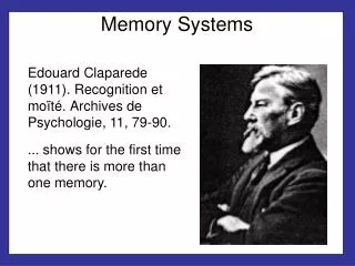
Memory Systems. Embedded Systems Design and Implementation Witawas Srisa-an. Agenda. Go over memory device and system Basic technology Review of memory organization Review of memory management Credits Materials presented in this slide set are from

E N D
Memory Systems Embedded Systems Design and Implementation Witawas Srisa-an
Agenda • Go over memory device and system • Basic technology • Review of memory organization • Review of memory management • Credits • Materials presented in this slide set are from • Steve Heath, Embedded Systems Design 2nd Ed., Newnes, Elsevier Science • Wayne Wolf, Computers as Components, Morgan Kaufman, Elsevier Science
Memory Technology • Volatile • DRAM • SRAM • Non-volatile • EPROM • EEPROM • Flash
Signals • Address bus • Data bus • Chip selects • Select chips from an array within a memory device • Control signals • Read/write
Dynamic RAM Technology • Used for cheap/large memory • Cost determines by the number of transistors/bit and packaging technology • How many per bit? • How many pins? • Need to refresh regularly (15 microseconds) • Why? • Result in 3 – 4% theoretical maximum processing overhead • Higher density • 4 to 5 more times than SRAM
DRAM Interface CE’ DRAM R/W’ RAS’ CAS’ Adrs Data
DRAM Interface • Two stages • Upper half of address is placed on the address bus to form row address then assert RAS signal • Then, lower half of address is placed on the address bus to form column address then assert CAS signal • Notice, row address is buffered internally • Access time from assertion of RAS to appearance of data
DRAM Interface CE’ R/W’ RAS’ CAS’ row adrs col adrs Adrs Data data time
DRAM Interface 256Kbit (512 bits/row 16 DRAMs) • Things to consider • memory chip (16K x 1 or 4K x 4) • the width of each row • the number of DRAM in the array
DRAM Interface 256Kbit (512 bits/row 16 DRAMs) 0 0 0 0 0 1 0 0 0 0 0 0 0 1 0 0 • Things to consider • memory chip (16K x 1 or 4K x 4) • the width of each row • the number of DRAM in the array
Page Mode DRAM • First access to a row, supply RAS • Afterward, keep RAS assert so only need to supply CAS • Performance gain is in cutting down the time needed to provide the RAS pulse • Not truly random access • 256 KB memory module (512 bit/row and 16 DRAMs in an array) • How large is a page? • Can be interleaved and/or burst mode
Page Mode DRAM 256Kbit (512 bits/row, 16 DRAMs, 4K x 4) 0 0 0 0 0 1 0 0 0 0 0 0 0 1 0 0 How big is a page?
Page Mode DRAM CE’ R/W’ RAS’ CAS’ row adrs col adrs col adrs col adrs Adrs Data data data data time
EDO RAM CE’ R/W’ RAS’ CAS’ row adrs col adrs col adrs col adrs Adrs Data data data data time
Video RAM • DRAM with shift register • Simultaneous accesses between processor and the video display • Shift register is driven by clock serially
Static RAM Technology • Used for fast/small memory • 4 to 5 transistors per bit • Need more resource • No refresh is needed • Example • Cache memory • Local memory-
SRAM Interface SRAM CE’ R/W’ Adrs Data
SRAM Interface CE’ R/W’ Adrs From SRAM From CPU Data read write time
SRAM vs DRAM (Pin) • How many pins are needed for a 1M x 1 • DRAM chip? • SRAM chip? CE’ SRAM DRAM CE’ R/W’ R/W’ RAS’ Adrs CAS’ Adrs Data Data
SRAM • Has been said to consume more power than DRAM • Only true during switching • Use less quiescent current than DRAM which has to be refreshed all the time • Can use battery to back-up SRAM
Non-Volatile Memory • EPROM • Read-only • Erasable through UV • Flash • Electrically erasable • Same access time as DRAM • EEPROM • Erase in block using electrical pulses
Basic Memory Organization • Processors don’t request data in a single bit. They request data in multiple bits • MC68000 has 16-bit data path • Either 16x1, 4x4 or 2x8 device would be needed • We have by 1, by 4, by 8 by 16 or more organization
Memory Packaging • Dual in line memory module (DIMM) • 64 bit • SIMM • 32 bit
OS Review • Why do we need memory management? • Relocation • Protection • Large address space • Trade offs • Slower memory access • Translation overhead • Additional storage for look-up tables