Download
1 / 23
230 likes | 353 Views
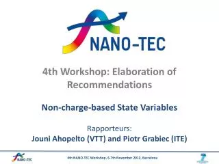
4th Workshop: Elaboration of Recommendations The ecosystem technology in beyond CMOS in Europe Rapporteurs : Alain Cappy (CNRS) and Thomas Swahn (Chalmers). WHICH ECOSYSTEM ?. Our scope: “Beyond CMOS” Information processing , memory, communications Our input comes from:

E N D
4th Workshop: Elaboration of Recommendations The ecosystem technology in beyond CMOS in Europe Rapporteurs: Alain Cappy (CNRS) and Thomas Swahn (Chalmers) 4th NANO-TEC Workshop, 6-7th November 2012, Barcelona
WHICH ECOSYSTEM ? • Our scope: “Beyond CMOS” • Information processing, memory, communications • Our input comes from: • all beyond-CMOS conclusions from NANO-TEC • + known activities in Europe • + electronics survey • + the NANO-TEC projects recommendations for the future 4th NANO-TEC Workshop, 6-7th November 2012, Barcelona
CONTEXT • A critical issue in beyond CMOS research is the availability of advanced technology. • The ecosystem technology has many players • A clear definition of the roles of the respective players is needed in order to avoid non-constructive competition and waste of resources 4th NANO-TEC Workshop, 6-7th November 2012, Barcelona
CONTEXT • The ecosystem technology has three main players with different access status • Academia (with an R&D horizon > 6 years, TRL 1-4) – basic understanding, test and validation of innovative architectures, materials and processes for future ICT. • Research Institutes (RTOs, Integration Centres with R&D horizon 3–6 years, TRL 3-7) – Technology implementation and the assessment towards Production Equipment; development of high performance components. • Industry (with R&D horizon < 3 years, TRL 6-9) – Technology research, innovation and exploitation; Process introduction and continuous improvement with innovative approaches (yield, reliability,…). 4th NANO-TEC Workshop, 6-7th November 2012, Barcelona
CONTEXT TRL metrics TRL 9 8 7 6 5 4 Overlapneeded to reduce the time to market 3 2 1 time Research institutes Main actors Industry Academia 4th NANO-TEC Workshop, 6-7th November 2012, Barcelona
CONTEXT Ecosystem aspects Regional Clusters RegionalEcosystem Regional Clusters RegionalEcosystem Large ResearchInstitutes Large Industry Large Industry RI Regional Clusters RegionalEcosystem RI Academia 4th NANO-TEC Workshop, 6-7th November 2012, Barcelona
BEYOND CMOS TECHNOLOGY ECOSYSTEM • Beyond CMOS address medium/long term technologies: the main players are academia and large research institutes. BUT the active role of Industry is mandatory: • to contribute to the identification of relevant long-term fundamental research topics needed in the value chain, • to define expectations for ultimate CMOS technology, applications, and services (> 2015), • to provide critical feedback to research institutes and academia. 4th NANO-TEC Workshop, 6-7th November 2012, Barcelona
BEYOND CMOS TECHNOLOGY ECOSYSTEM 4th NANO-TEC Workshop, 6-7th November 2012, Barcelona
BEYOND CMOS DEVICE TECHNOLOGIES? • Using the three device categories chosen for workshop 4, we can describe a little bit the technology state of the art and the needs to push the technology forward. • Digital with charge as state variable (New semiconductor transistor ( TFET,i-MOS, III-V, nanowire…but also nanomechanical switch). Generally , the demonstration is carried out for a single device or low complexity circuits. To demonstrate better performance than CMOS (at least for one or two parameters), manufacturability is a key question. So the main difficulty is the access to large scale infrastructures (LSI) at reasonable cost. Design is not a problem if the new device can simply replace CMOS 4th NANO-TEC Workshop, 6-7th November 2012, Barcelona
BEYOND CMOS DEVICE TECHNOLOGIES? • Digital with state variable other than charge (Spin, molecular state….) For this domain, the objective is mainly to demonstrate the possibility to use of a new two state device to make digital circuits. Manufacturability on a semiconductor process line is a key question. • Non digital (quantum, neuromorphic). For this domain, the notion of device is not relevant. Completely new technology ( self assembly ….) can be proposed for which the technology ecosystem is not clear. 4th NANO-TEC Workshop, 6-7th November 2012, Barcelona
Bottom-up infrastructurenetworking and mapping • A grass-root mapping approach to European infrastructures >≈ 500 m2 • to connect small ecosystems (typically small RI, regional networks) to large institutes and industry • Bottom-up and open access approach: several coordinated proposals submitted (Myfab, NorFab, RENATECH, TRAIN2-network etc.) to the EU-open consultation (22 October). • Not the complete picture – but the NANO-TEC map of our extended infrastructure network (inclusive approach) • Additional input to the final report wanted! 4th NANO-TEC Workshop, 6-7th November 2012, Barcelona
EuropeanInfrastructureNetwork • NorFab, Norway, (4 labs) • Finland, VTT, Finland • Myfab, Sweden (3 labs) • Danchip, Denmark • Tyndall, Ireland • NanoLabNL, Holland • Twente, The Netherlands • U. Southampton, England • UC Lovain, Belgium • FZ Jüelich, Germany • IMTEK/HSG-IMITGermany • ITE, Poland • RENATEC, France (6 labs) • EPFL, Switzerland • NANOLOTO, Spain(x labs) • IMEL Demokritos, Greece • INESC NM, Portugal • INL, Portugal 15 NANOLITO-netw. 12 ITE, Poland 3 Myfab, 3 labs 17 INESC NM 1 NorFab 4 labs 5Tyndall 14 EPFL 13 RENATEC Network, 6labs 2 VTT 6NanoLab NL 4 DTU Danchip 18 INL 9-11 FZ Jüelich, IMTEK (6 labs) 7 U Southampton 8 UC Lovain WINFAB 16 IMEL Demokritos
HOW TO IMPROVE THE BEYOND CMOS TECHNOLOGY ECOSYSTEM ? • What is the opinions of the players? • The NANOTEC electronic poll: • Posted in the NANO-TEC website July – August 2012 • Invitations sent to experts within the extended • NANO-TEC network • 19 replies registered 4th NANO-TEC Workshop, 6-7th November 2012, Barcelona
Opinion on the general ”beyond CMOS” Europeancapabilities …
HOW TO IMPROVE THE BEYOND CMOS TECHNOLOGY ECOSYSTEM ? • European research is strong in beyond CMOS technologies, but the transition from ideas arising from basic research to competitive product is a weak link in European nanoelectronics value chains • The gap between basic knowledge generation and the subsequent commercialisation of this knowledge in marketable products is known as the "valley of death" issue. Pilot lines Industrial facilities academic facilities Knowledge Market Valley of death
HOW TO IMPROVE THE BEYOND CMOS TECHNOLOGY ECOSYSTEM ? • Make a better connection between the three pillars • The first pillar, “academic facilities” consists of taking best advantage of European scientific excellence in transforming the ideas arising from fundamental research into technologies competitive at world level. Proofs of concept and patents • The second pillar, “Pilot lines” consists of putting in place pilot lines having technology prototyping facilities to enable the fabrication of innovative prototypes. • The third pillar, “Industrial facilities” starting from product prototypes duly validated during the demonstration phase to create and maintain in Europe attractive economic
HOW TO IMPROVE THE BEYOND CMOS TECHNOLOGY ECOSYSTEM ? • Many structures already exist (CATRENE, prins, ENIAC, AENAS, SINANO, ENI2, Silicon Europe, …) gathering the same communities. • DO NOT create a new one • How to improve the ecosystem without increased complexity ??
RECOMMENDATIONS • The first recommendation: • Academic networking • We propose that Europe organize all the advanced academic technological facilities having a significant activity in beyond CMOS research in a European network with one and only one entry point in each country, each entry point having mission to represent/structure its national facilities • Do not make the picture more complicated! • In order to avoid a new structure, it should be useful that this network could be managed by an existing initiative. This network will be complementary to the facilities of the RTO and tightly link to them in order to allow a smooth crossing of the ‘valley of death’. 4th NANO-TEC Workshop, 6-7th November 2012, Barcelona
RECOMMENDATIONS Academic facility European network 4th NANO-TEC Workshop, 6-7th November 2012, Barcelona
RECOMMENDATIONS The second recommendation: Beyond CMOS education We propose that Europe should create a multidisciplinary ‘Beyond CMOS ‘ Erasmus Mundus programme to educate a new generation of student to future information processing concepts: theory of information, binary and non binary information processing, quantum computing, neuromophic computing. Feedback from Industry The low level of feedback from industry is also a weakness in Europe. It is recommended that industry will define more clearly the expectations for ultimate current technology, future needs and roadmaps of long-term research. This feedback would increase the manpower on research on subjects that are considered as strategic by industry for the long term and avoid dispersion on subjects of minor importance. 4th NANO-TEC Workshop, 6-7th November 2012, Barcelona