Download
1 / 24
240 likes | 369 Views
GEOMETRIC RELIEF OF STRAINED GaAs ON NANO-SCALE GROWTH AREA. J. H. Woo, Department of Electrical & Computer Engineering Texas A&M University. Table of Contents. INTRODUCTION BASIC PHYSICS ON EPITAXY SAMPLE DESCRIPTION RESULTS DISCUSSIONS FUTURE DEVELOPMENT CONCLUSIONS. Introduction.

E N D
GEOMETRIC RELIEF OF STRAINED GaAs ON NANO-SCALE GROWTH AREA J. H. Woo, Department of Electrical & Computer Engineering Texas A&M University
Table of Contents • INTRODUCTION • BASIC PHYSICS ON EPITAXY • SAMPLE DESCRIPTION • RESULTS • DISCUSSIONS • FUTURE DEVELOPMENT • CONCLUSIONS
Introduction • Scaling of silicon technology is near the end of its lifetime • The newest Intel’s processor is fabricated with 32nm nodes • 22 nm in 2011, 16 nm in 2013 and 11 nm in 2016 • Then what? • Faster performing device is needed • III-V devices have been proposed • Higher electron mobility of GaAs can improve the speed of the transistors built on it
Introduction • Problems with III-V electron devices • Substrate cost is much higher than Si • Growth of III-V on Si is difficult and usually defective • For example, GaAs has 4% lattice mismatch to Si
Introduction • Problems with GaAs epitaxy on Si • No defect-free GaAs growth has been experimentally demonstrated. • 4% misfit indicates that one dislocation will be occupied in every 25 atomic planes1 • Ge has almost the same lattice parameter as GaAs and its critical thickness (hc) is ~2 nm on Si2 • Ge is the optimum case as it is a unary material • For binary materials, single crystal epitaxy is more defective and therefore, the critical thickness is higher.
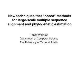
Introduction • Proposed work • Epitaxial layer in a metastable state caused by strain may be able to extend the critical thickness • Study by Majhi, et. al. shows that Ge layer at metastable state showed higher critical thickness (Fig. 1) • GaAs growth on a limitedarea to relief the strainat the edge may helpto increasehc. Figure 1. Dependence of critical thickness on the stability state2
Thin Film Epitaxy and Applications • Epitaxy • The growth of a crystal of one material on the crystal face of another material in such a way that both materials have the same or similar structural orientation. • Applications of GaAs Epitaxy • Solar cells • Semiconductor Lasers • High mobility devices
Lattice Mismatch • Pseudomorphic growth: one-to-one matching • Films strained due to misfit • Misfit dislocation occurs with large strain • ε// =(as-af)/af • ε⊥ =(af⊥ -af)/af where af⊥ = as3/af2 • Misfit %, • Lattice mismatched when f is small
Strain/Stress in Thin Films • Mismatch means stress. • af>as => film in compression, subs in tension • as>af => film intension, subs in compression
Defects • Formed during the relaxation of excessive strain. • Among many defect types, we are interested in dislocations
Critical Thickness • The maximum thickness before relaxation of strain occurs leading to dislocations
SAMPLE DESCRIPTION • Various thicknesses of GaAs was selectively grown on (110) surface of Si • 20Å, 40Å, 80Å and 100Å • The geometry of GaAs epitaxial site is limited to a long, narrow channel • 20 nm in width and semi-infinitely long
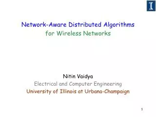
Fabrication Method • Number of possible fabrication method can be used • The easiest method is to start from (110) Si substrate • (110) Si is patterned into long, narrow patterns using electron lithography • The direction of this pattern was oriented so that (001) surface is exposed on the side • The patterned substrate is RIE etched to isolate the epitaxy site • GaAs is selectively grown on (110) surface only using an MBE system • The thickness is controlled carefully so that each batch of sample has GaAs thickness of 20 Å to 100 Å
Fabrication Method Si (a) (b) GaAs (c) Figure 2. Fabrication steps. (a) (110) Si, (b) Si patterned and RIE etched, (c) GaAs is selectively MBE grown on (110) surface
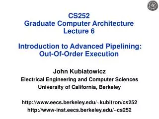
Strain on GaAs and Si • Lattice parameters • GaAs – 5.65 Å • Si – 5.43 Å • Si will be under tensile strain and GaAs under compressive strain due to their lattice parameters GaAs Si Figure 3. Strain direction
Strain Simuation • A study shows an equation which calculates the stress on the SiGe film on Si3
Strain Simuation σ_bar : effective stress σx : normal stress μf : Young’s Modulus for film μs : Young’s Modulus for substrate vf : Poisson’s ratio for filmvs: Poisson’s ratio for substrate A : x dimension of epitaxy layer B : y dimension of epitaxy layer a : x position b : y position f(a) : stress as a function of position in x f(b) : stress as a function of position in y h : thickness of epitaxy layer
Results • A defect-free single crystal layer of GaAs at 20 Å of thickness has been demonstrated Figure 4. defect-free single crystal 20-Å thick GaAs is grown on Si
Results • Epi-layers with larger thicknesses showed numerous dislocations at 60° to the surface Figure 5. defective GaAs epitaxial layers at a larger thickness
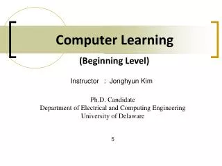
Discussions • The simulation result shows the relieving effect of the edges • The average stress along the x direction was approximately 95% of the original stress, yielding 5% of stress relief due to the finite epitaxial site Figure 6. effective stress plot
Discussions • We can deduce that the 5% reduction in the stress was able to effectively reduce the strain in the film so that higher critical thickness can be achieved. • This led to the phenomenal result of the demonstration of growing defect-free single crystalline GaAs on Si • This could open up the research opportunity for higher performance electron devices
Future Research • Assuming that GaAs can now be successfully grown on Si, we can now design a GaAs device on Si and analyze the performance of such device • Synopsys Sentaurus TCAD can simulation 1D/2D/3D devices. The future research will involve the simulation using this software
Conclusion • Defect-free single crystalline GaAs was successfully grown on Si at a very small thickness but this could still lead to an opportunity for future electron devices as well as other applications • The simulation shows that the edge effect could reduce the stress on the film by 5% and this effectively led to an increase in the critical thickness of GaAs epitaxy on Si
References • Fischer, R., Morkoc, H., Neumann, D. A., Zabel, H., Choi, C., Otsuka, N., Longerbone, M., and Erickson, L. P., Journal of Applied Physics 60 (5) 1986. • P. Majhi, P. Kalra, R. Harris, K. J. Choi, D. Heh, J. Oh, D. Kelly, R. Choi,B. J. Cho, S. Banerjee, W. Tsai, H. Tseng, and R. Jammy, IEEE Electron Device Letters, 29 (1) 2008. • Fischer, A., Richter, H., Applied Physics Letters, 61 (22) 1992.