Download
1 / 11
130 likes | 278 Views
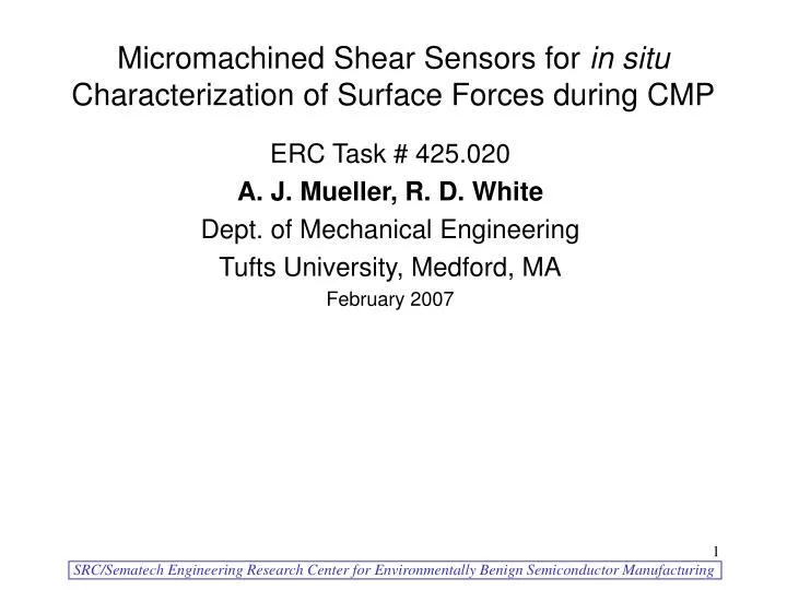
Micromachined Shear Sensors for in situ Characterization of Surface Forces during CMP. ERC Task # 425.020 A. J. Mueller, R. D. White Dept. of Mechanical Engineering Tufts University, Medford, MA February 2007. Project Objectives.

E N D
Micromachined Shear Sensors for in situ Characterization of Surface Forces during CMP ERC Task # 425.020 A. J. Mueller, R. D. White Dept. of Mechanical Engineering Tufts University, Medford, MA February 2007
Project Objectives • Fabricate and implement micromachined shear stress sensors for characterization of surface forces during chemical-mechanical polishing (CMP). • Measure local, real-time shear stress at the pad-wafer interface during CMP due to slurry and asperity interactions with the wafer. Polishing Pad Asperity Fluid Forces Polydimethylsiloxane (PDMS) Surface Structures deflect to indicate shear forces present Asperity Forces Substrate
Environmental Safety and Health (ESH)Metrics and Impacts METRICIMPACT Energy Consumption During Understanding wafer-pad Process interactions during polish leads to reduced time to polish and tool energy consumption DI Water Consumption During Optimized process parameters based Process on in-situ characterization of contact, and forces leads to reduced time to Process Chemical Consumption polish and slurry consumption (Slurry Chemicals) optimization
Sensor Process & Design Overview • Initial Design • 85 µm high posts: successful • 80, 90, 100 µm diameter: successful • 10, 15, 20 µm : not fully formed; incomplete formation of mold • Final Design • Fabrication limits for final design: 30-40 µm minimum diameter at 85-100 µm high. • Camera resolution: 5-10 µm deflection • Dyeing may improve resolution Light microscope image of SU-8 mold from design 1 Design 1 CAD Layout Si Substrate ~100 µm SU-8 Photoresist Expose/Develop = SU-8 mold SEM image of SU-8 mold from design 1 SEM image of PDMS structure from design 1 Pour/Cure PDMS onto SU-8 mold Final Design 30 µm 100um diameter posts Calibration block
Mounting Without dye: 80-100 µm structures visible. Expect to be able to resolve ~5-10 µm displacement with existing optics. Viewing Area (radially symmetric) CMP Axle ABS Plastic Pressure Fit Acrylic ‘Windows’ Adhesive Pyrex Wafer Covalent Bond through O2 plasma ashing PDMS sensor Sensors seen through acrylic viewing window, Pyrex, and the back of the PDMS wafer Imaging Current Optics Rhodamine B With dye: some edges are very bright. Additional experiments are planned to attempt to achieve uniform edge dyeing.
Asperity Force Estimations Total shear force load is COF·Downforce·Wafer Area (for 4” wafer) ≈ 0.5 (1.8 psi) (p (50 mm)2)≈ 50 N Number of Asperities in Contact: Wafer Area/Asperity Neighborhood Area (for 4” wafer) ≈ (p (50 mm)2)/ ((30 µm)2) ≈ 8.7 · 106asperity contacts/wafer Option #1 : Assume 30 µm center to center spacing on asperity tips with a square grid. Force per asperity is total force over number of asperities ≈ 50 N/(8.7·106 asperities) ≈ 6 mN Estimate of static wafer contact % area for IC1000 pad at 1.8 psi downforce is 0.7%. Option #2 : Determine number of contacts based on ratio of total contact area to individual asperity contact area. ~20µm ≈ p(5 µm)2 ≈ 80 µm2 Number of Asperities in Contact: ≈ (0.007·p (50 mm)2)/ 80 µm2 ≈ 6.9 · 105asperity contacts/wafer • Carolina L. Elmufdi and Gregory P. Muldowney, “The Impact of Pad Microtexture The Impact of Pad Microtexture and Material Properties and Material Properties on Surface Contact and Defectivity in CMP on Surface Contact and Defectivity in CMP” Force per asperity is total force over number of asperities ≈ 50 N/(6.9·105 asperities) ≈ 70 µN
Expected Sensitivities and Deflections Estimated Fluid Forces Estimated Structure Stiffness Estimated Sensitivities L=85 µm Eestimated=750 kPa Deflections due to asperity forces are expected to be at least 5x to 100x larger than deflections due to fluid forces.
Preliminary Sensor Calibrations Horizontal Distance (um) Calculated Post Deflections @ varying locations along the post Dektak Downforces Dektak Tip Paths Post Deflection (um) Post Deflection (µm) Total Deflection (y) = Δ + Fi/k Δ – Deflection due to sample tilt PDMS Post Downforce (µN) Nonlinearity of post deflections (60 µm from the post base) Calculated stiffness at 60 µm from the base= 3.1 N/m (σ = 0.63) ~10% of the value estimated from beam theory Post Deflection (µm) Non-linearity at 60 µm from the post base with a downforce of 100 µN is around 5% Downforce (µN)
Future Plans • Develop experimental apparatus for calibrating post deflection under known: • Fluid flow loads • Mechanical loads • Improve dyeing ability to improve optical post resolution. • Integrate with CMP rig for in situ surface force measurements.
Industrial Collaboration/Technology Transfer • Close collaboration with industry partners – Cabot Microelectronics and Intel • Monthly telecons – secure website for information exchange • Semi-annual face-to-face meetings • Thesis committees and joint publication authorship • Metrology and analysis methodology technology transfer • In-kind support – specialized supplies and equipment • Student internships (e.g. C. Gray at Intel during Summer 2005) • Close coordination with A. Philipossian research group at U of Arizona • Information and results exchange with MIT (D. Boning) • ERC project • Monthly joint meetings of PIs and research students • Discussion of findings with other colleagues (e.g. E. Paul – Stockton College on leave at MIT)
Conclusions • The sensors developed will allow measurement of shear forces during CMP at an estimated force resolution of 1-100 µN and spatial resolution of 300 µm. • Sensor fabrication feasibility has been proven and diameter limitations have been established at 30 µm. • Calibration and implementation of the shear sensors are ongoing.