Download
1 / 36
360 likes | 596 Views
Memory Technology March 14, 2000. 15-213. Topics Memory Hierarchy Basics Static RAM Dynamic RAM Magnetic Disks Access Time Gap. class17.ppt. Computer System. Processor. Reg. Cache. Memory-I/O bus. I/O controller. I/O controller. I/O controller. Memory. Display. Network. Disk.

E N D
Memory TechnologyMarch 14, 2000 15-213 • Topics • Memory Hierarchy Basics • Static RAM • Dynamic RAM • Magnetic Disks • Access Time Gap class17.ppt
Computer System Processor Reg Cache Memory-I/O bus I/O controller I/O controller I/O controller Memory Display Network Disk Disk
CPU C a c h e regs Levels in Memory Hierarchy cache virtual memory Memory disk 8 B 32 B 8 KB Register Cache Memory Disk Memory size: speed: $/Mbyte: block size: 200 B 2 ns 8 B 32KB - 4MB 4 ns $100/MB 32 B 128 MB 60 ns $1.50/MB 8 KB 20 GB 8 ms $0.05/MB larger, slower, cheaper
Scaling to 0.1µm • Semiconductor Industry Association, 1992 Technology Workshop • Projected future technology based on past trends • 199219951998200120042007 • Feature size: 0.5 0.35 0.25 0.18 0.12 0.10 • Industry is slightly ahead of projection • DRAM capacity: 16M 64M 256M 1G 4G 16G • Doubles every 1.5 years • Prediction on track • Chip area (cm2):2.5 4.0 6.0 8.0 10.0 12.5 • Way off! Chips staying small
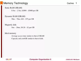
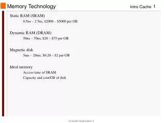
Static RAM (SRAM) • Fast • ~4 nsec access time • Persistent • as long as power is supplied • no refresh required • Expensive • ~$100/MByte • 6 transistors/bit • Stable • High immunity to noise and environmental disturbances • Technology for caches
bit line bit line Stable Configurations b b’ word line (6 transistors) 0 1 1 0 Anatomy of an SRAM Cell Terminology: bit line: carries data word line: used for addressing • Write: • 1. set bit lines to new data value • b’ is set to the opposite of b • 2. raise word line to “high” • sets cell to new state (may involve flipping relative to old state) • Read: • 1. set bit lines high • 2. set word line high • 3. see which bit line goes low
1 0.9 0.8 0.7 0.6 0.5 V1 0.4 V2 0.3 0.2 Vin 0.1 V1 0 0 0.2 0.4 0.6 0.8 1 V2 Vin SRAM Cell Principle • Inverter Amplifies • Negative gain • Slope < –1 in middle • Saturates at ends • Inverter Pair Amplifies • Positive gain • Slope > 1 in middle • Saturates at ends
Vin V1 V2 1 0.9 0.8 0.7 0.6 0.5 Vin 0.4 V2 0.3 0.2 0.1 0 0 0.2 0.4 0.6 0.8 1 Vin Bistable Element • Stability • Require Vin = V2 • Stable at endpoints • recover from pertubation • Metastable in middle • Fall out when perturbed • Ball on Ramp Analogy Stable Metastable Stable
Address decoder A0 A1 A2 A3 Example SRAM Configuration (16 x 8) b7 b7’ b1 b1’ b0 b0’ W0 W1 memory cells W15 R/W sense/write amps sense/write amps sense/write amps Input/output lines d7 d1 d0
Dynamic RAM (DRAM) • Slower than SRAM • access time ~60 nsec • Nonpersistant • every row must be accessed every ~1 ms (refreshed) • Cheaper than SRAM • ~$1.50 / MByte • 1 transistor/bit • Fragile • electrical noise, light, radiation • Workhorse memory technology
Reading Word Line Bit Line V ~ Cnode / CBL Anatomy of a DRAM Cell Word Line Bit Line Storage Node Access Transistor Cnode CBL Writing Word Line Bit Line V Storage Node
c r Addressing Arrays with Bits • Array Size • R rows, R = 2r • C columns, C = 2c • N = R * C bits of memory • Addressing • Addresses are n bits, where N = 2n • row(address) = address / C • leftmost r bits of address • col(address) = address % C • rightmost bits of address • Example • R = 2 • C = 4 • address = 6 row col address = n 0 1 2 3 0 000 001 010 011 1 100 101 110 111 col 2 row 1
8 \ 8 \ Example 2-Level Decode DRAM (64Kx1) RAS 256 Rows Row decoder 256x256 cell array Row address latch row 256 Columns A7-A0 column sense/write amps R/W’ col Provide 16-bit address in two 8-bit chunks Column address latch column latch and decoder CAS Dout Din
DRAM Operation • Row Address (~50ns) • Set Row address on address lines & strobe RAS • Entire row read & stored in column latches • Contents of row of memory cells destroyed • Column Address (~10ns) • Set Column address on address lines & strobe CAS • Access selected bit • READ: transfer from selected column latch to Dout • WRITE: Set selected column latch to Din • Rewrite (~30ns) • Write back entire row
Observations About DRAMs • Timing • Access time (= 60ns) < cycle time (= 90ns) • Need to rewrite row • Must Refresh Periodically • Perform complete memory cycle for each row • Approximately once every 1ms • Sqrt(n) cycles • Handled in background by memory controller • Inefficient Way to Get a Single Bit • Effectively read entire row of Sqrt(n) bits
RAS Row decoder 256x256 cell array Row address latch 8 \ row A7-A0 sense/write amps R/W’ col Column address latch column latch and decoder 8 \ CAS Enhanced Performance DRAMs • Conventional Access • Row + Col • RAS CAS RAS CAS ... • Page Mode • Row + Series of columns • RAS CAS CAS CAS ... • Gives successive bits • Other Acronyms • EDORAM • “Extended data output” • SDRAM • “Synchronous DRAM” Entire row buffered here Typical Performance row access time col access time cycle time page mode cycle time 50ns 10ns 90ns 25ns
256x256 cell array column sense/write amps Shift Register Video RAM • Performance Enhanced for Video / Graphics Operations • Frame buffer to hold graphics image • Writing • Random access of bits • Also supports rectangle fill operations • Set all bits in region to 0 or 1 • Reading • Load entire row into shift register • Shift out at video rates • Performance Example • 1200 X 1800 pixels / frame • 24 bits / pixel • 60 frames / second • 2.8 GBits / second Video Stream Output
DRAM Driving Forces • Capacity • 4X per generation • Square array of cells • Typical scaling • Lithography dimensions 0.7X • Areal density 2X • Cell function packing 1.5X • Chip area 1.33X • Scaling challenge • Typically Cnode / CBL = 0.1–0.2 • Must keep Cnode high as shrink cell size • Retention Time • Typically 16–256 ms • Want higher for low-power applications
Plate Area A Dielectric Material Dielectric Constant d C = A/d DRAM Storage Capacitor • Planar Capacitor • Up to 1Mb • C decreases linearly with feature size • Trench Capacitor • 4–256 Mb • Lining of hole in substrate • Stacked Cell • > 1Gb • On top of substrate • Use high dielectric
SiO2 Dielectric Storage Plate Reference Plate Trench Capacitor • Process • Etch deep hole in substrate • Becomes reference plate • Grow oxide on walls • Dielectric • Fill with polysilicon plug • Tied to storage node
IBM DRAM Evolution • IBM J. R&D, Jan/Mar ‘95 • Evolution from 4 – 256 Mb • 256 Mb uses cell with area 0.6 µm2 Cell Layouts 4Mb 4 Mb Cell Structure 16Mb 64Mb 256Mb
Mitsubishi Stacked Cell DRAM • IEDM ‘95 • Claim suitable for 1 – 4 Gb • Technology • 0.14 µm process • Synchrotron X-ray source • 8 nm gate oxide • 0.29 µm2 cell • Storage Capacitor • Fabricated on top of everything else • Rubidium electrodes • High dielectric insulator • 50X higher than SiO2 • 25 nm thick • Cell capacitance 25 femtofarads Cross Section of 2 Cells
Magnetic Disks Disk surface spins at 3600–7200 RPM read/write head arm The surface consists of a set of concentric magnetized rings called tracks The read/write head floats over the disk surface and moves back and forth on an arm from track to track. Each track is divided into sectors
Disk Capacity • Parameter 18GB Example • Number Platters 12 • Surfaces / Platter 2 • Number of tracks 6962 • Number sectors / track 213 • Bytes / sector 512 • Total Bytes 18,221,948,928
Disk Operation • Operation • Read or write complete sector • Seek • Position head over proper track • Typically 6-9ms • Rotational Latency • Wait until desired sector passes under head • Worst case: complete rotation 10,025 RPM 6 ms • Read or Write Bits • Transfer rate depends on # bits per track and rotational speed • E.g., 213 * 512 bytes @10,025RPM = 18 MB/sec. • Modern disks have external transfer rates of up to 80 MB/sec • DRAM caches on disk help sustain these higher rates
Disk Performance • Getting First Byte • Seek + Rotational latency = 7,000 – 19,000 µsec • Getting Successive Bytes • ~ 0.06 µsec each • roughly 100,000 times faster than getting the first byte! • Optimizing Performance: • Large block transfers are more efficient • Try to do other things while waiting for first byte • switch context to other computing task • processor is interrupted when transfer completes
Disk / System Interface (1) Initiate Sector Read • 1. Processor Signals Controller • Read sector X and store starting at memory address Y • 2. Read Occurs • “Direct Memory Access” (DMA) transfer • Under control of I/O controller • 3. I/O Controller Signals Completion • Interrupts processor • Can resume suspended process Processor Reg (3) Read Done Cache Memory-I/O bus (2) DMA Transfer I/O controller Memory Disk Disk
Magnetic Disk Technology • Seagate ST-12550N Barracuda 2 Disk • Linear density 52,187. bits per inch (BPI) • Bit spacing 0.5 microns • Track density 3,047. tracks per inch (TPI) • Track spacing 8.3 microns • Total tracks 2,707. tracks • Rotational Speed 7200. RPM • Avg Linear Speed 86.4 kilometers / hour • Head Floating Height 0.13 microns • Analogy: • put the Sears Tower on its side • fly it around the world, 2.5cm above the ground • each complete orbit of the earth takes 8 seconds
CD Read Only Memory (CDROM) • Basis • Optical recording technology developed for audio CDs • 74 minutes playing time • 44,100 samples / second • 2 X 16-bits / sample (Stereo) Raw bit rate = 172 KB / second • Add extra 288 bytes of error correction for every 2048 bytes of data • Cannot tolerate any errors in digital data, whereas OK for audio • Bit Rate • 172 * 2048 / (288 + 2048) = 150 KB / second • For 1X CDROM • N X CDROM gives bit rate of N * 150 • E.g., 12X CDROM gives 1.76 MB / second • Capacity • 74 Minutes * 150 KB / second * 60 seconds / minute = 650 MB
metric 1980 1985 1990 1995 2000 2000:1980 $/MB 19,200 2,900 320 256 100 190 access (ns) 300 150 35 15 2 100 SRAM metric 1980 1985 1990 1995 2000 2000:1980 $/MB 8,000 880 100 30 1.5 5,300 access (ns) 375 200 100 70 60 6 typical size(MB) 0.064 0.256 4 16 64 1,000 DRAM metric 1980 1985 1990 1995 2000 2000:1980 $/MB 500 100 8 0.30 0.05 10,000 access (ms) 87 75 28 10 8 11 typical size(MB) 1 10 160 1,000 9,000 9,000 Disk Storage Trends (Culled from back issues of Byte and PC Magazine)
Processor clock rates Processors metric 1980 1985 1990 1995 2000 2000:1980 typical clock(MHz) 1 6 20 150 600 600 processor 8080 286 386 Pentium P-III culled from back issues of Byte and PC Magazine
Memory Technology Summary • Cost and Density Improving at Enormous Rates • Speed Lagging Processor Performance • Memory Hierarchies Help Narrow the Gap: • Small fast SRAMS (cache) at upper levels • Large slow DRAMS (main memory) at lower levels • Incredibly large & slow disks to back it all up • Locality of Reference Makes It All Work • Keep most frequently accessed data in fastest memory