Download

1 / 51
520 likes | 740 Views
Instrumentation. Summary of previous slides : We now know how most particles ( i.e all particles that live long enough to reach a detector; e,u,p, ,k,n, , neutrinos,etc) react with matter.

E N D
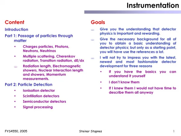
Instrumentation Summary of previous slides : We now know how most particles ( i.e all particles that live long enough to reach a detector; e,u,p,,k,n,, neutrinos,etc) react with matter. We now know how to identify particles to some extend, how to measure E and p, v, and how to measure lifetimes using secondary vertices, etc • Lecture set 2 : but we skipped one essential step in the process ….. • How are reactions of the various particles with detectors turned into electrical signals. We would like to extract position and energy information channel by channel from our detectors. • Three effects are usually used : • 1 Ionisation • 2 Scintillation • 3 Semi Conductors • and these are used in either for tracking, energy measurements, photon detectors for Cherenkov or TRT, etc • 4 Finally we will have a quick look at how electrical signals are amplified in FE electronics • and from then on it is all online (trigger, DAQ) and offline treatment and analysis …. Steinar Stapnes
Ionisation Detectors From CERN-CLAF, O.Ullaland Approximate computed curves showing the percentage of electron energy going to various actions at a given X/p (V/cm/mmHg) Elastic: loss to elastic impact Excitation: excitation of electron levels, leading to light emission and metastable states Ionization: ionization by direct impact Kinetic: average kinetic energy divided by their “temperature” Vibration: energy going to excitation of vibrational levels Add a sprinkling of argon L. B. Loeb, Basic Processes of Gaseous Electronics Steinar Stapnes
Ionisation Detectors Experimental results. Rare gases. Experimental results. Diatomic molecules. D. Rapp et al., Journal of Chemical Physics, 43, 5 (1965) 1464 Steinar Stapnes
Ionisation Detectors Fig 1. Ionisation potiential. The work required to remove a given electron from its orbit and place it at rest at an infinite distance. Fig 2. Note that limited number of primary electrons/ions. Fig 3 (table). Taking into account that some of the primary electrons will ionise further (factor 3-4 increase); nevertheless keep in mind that electronics noise can be 300-500 ENC. CRC Handbook 63 ed. From C.Joram Steinar Stapnes
Ionisation Detectors The different regions : Recombination before collection. Ionisation chamber; collect all primary charge. Flat area. Proportional counter (gain to 106); secondary avalanches need to be quenched. Limited proportionality (secondary avalanches distorts field, more quenching needed). Geiger Muller mode, avalanches all over wire, strong photoemission, breakdown avoided by cutting HV. Steinar Stapnes
Ionisation Detectors From C.Joram Steinar Stapnes
Ionisation Detectors Drift of electrons under the action of the electric field (superimposed on thermal movements) : The drift velocity of the positive ions under the action of the electric field is linear with the reduced electric field (E/pressure) up to very high fields. v +ions = +ions E where + 1/p and diffusion D+ions +ions T in CO2 with E=104 V/cm From CERN-CLAF, O.Ullaland Steinar Stapnes
Ionisation Detectors The amplification process : Let a-1 be the mean free path (also called the first Townsend coefficient) between each ionization, in other words dn = nadx. The gas amplification is then given by : From CERN-CLAF, O.Ullaland Korff’s approximation (model) where A and B are gas dependent constants and p is the pressure. for a gas mixture of Ar/CO2 : 80/20 Steinar Stapnes
Ionisation Detectors Cathode :A metallic cylinder of radius b Anode : A gold plated tungsten wire of radius a a = 10-5 m b/a = 1000 The formation of signal can be understood as follows. The electrostatic energy of the configuration is : where C is the capacitance per unit length of the configuration and l is the length. The potential energy of a charged particle at radius r is given by the charge times the potential : The result is an equation for how the voltage (signal) changes when the particle moves in the electric field : Anode Cathode Steinar Stapnes
Ionisation Detectors Signal induced by (mainly) the positive ions created near the anode. Assume that all charges are created within a distance from the anode. is of the order of a few 10’s of µm v electron = v ion /100 which can be seen from the equations below setting in the correct values for a and b : Assuming a=0 and all the signal comes from the ions we can write: r(t) can be taken from : The final result for v(t) : Steinar Stapnes
Ionisation Detectors In modern fast ionisation detectors the electrons are used (faster) as well as the beginning of the ion signal. For example if we use 5% of the signal with a gain 104 we still have a healthy signal compared to the noise – and we can operate mostly with the fast part of the signal (electrons) and differentiate away the tails …. Steinar Stapnes
Ionisation Detectors With these tools, we can now make : Straw Tube Multiwire Proportional Chambers Drift Chambers Time Projection Chambers Thin Gap Chambers Jet Chambers etc From CERN-CLAF, O.Ullaland Classic Multi-Wire Proportional Chamber (MWPC) Typical parameters : l : 5 mm s : 2 - 4 mm d : 20 mm Still possible to calculate by hand (leave as exercise for you) : and Steinar Stapnes
Ionisation Detectors Vs(z) x (mm) y (mm) Advanced calculations of electric field, drift, diffusion and signal formation can be done with Garfield. Two dimensional readout can be obtained by; crossed wires, charge division with resistive wires, measurement of timing differences or segmented cathode planes with analogue readout Resolution given by (binary readout) : Analogue readout and charge sharing can improve this significantly when the left/right signal size provide more information about the hit position. From Leo Steinar Stapnes
Resolution Charge on a single wire/strip is the worst possible situation for the resolution: 1 2 3 With analogue readout and charge sharing we improve the information content significantly – on the left we know that the hit was between the second and third readout electrode and closest to the 2nd, so we can make a probability function which is much more narrow (some times pitch/10).Another way of saying it: For every point between wire/strip 2 and 3 there is a unique value of : (Q2-Q3)/(Q2+Q3), so by measuring this quantity we can reconstruct the position. 1 2 3 Steinar Stapnes
Ionisation Detectors From C.Joram Drift Chambers : Reduced numbers of readout channels Distance between wires typically 5-10cm giving around 1-2 s drift-time Resolution of 50-100m achieved limited by field uniformity and diffusion More problems with occupancy Steinar Stapnes
Ionisation Detectors Time projection chamber : Drift to endplace where x,y are measured Drift-time provides z Analogue readout provide dE/dx Magnetic field provide p (and reduce transverse diffusion during drift) From Leo Steinar Stapnes
Ionisation Detectors From Leo Steinar Stapnes
In recent years there has been several developments directed towards making gas detectors more suitable for high rate applications (inner detectors components for LHC). I will mention only two (C.Joram; CERN summer student lectures 2002) : Steinar Stapnes
GEM : Gas Electron Multiplier Can be used as a detector on its own or as amplifier stage in multiple structure Steinar Stapnes
Scintillators • Scintillators are used in many connections : • Calorimetry (relatively cheap and good energy resolution) • Tracking (fibres) • Trigger counters • Time of flight • Veto Counters • Will discuss mainly inorganic (often used in calorimeters due to high density and Z; slow but high light output and hence good resolution) and organic (faster but less light output) • Will discuss readout (wavelength shifters, photon detectors and new developments to increase granularity of the readout). Steinar Stapnes
From CERN-CLAF, O.Ullaland Scintillators Inorganic Crystalline Scintillators The most common inorganic scintillator is sodium iodide activated with a trace amount of thallium [NaI(Tl)], Energy bands in impurity activated crystal http://www.bicron.com. Strong dependence of the light output and the decay time with temperature. Steinar Stapnes
Parameters for some common scintillator materials NaI has a light output of typically 40000 photons per MeV; keep in mind that light collection, and the quantum efficiency of the photo detector will reduce the signal significantly. The detector response is fairly linear (see Leo). Steinar Stapnes
Scintillators Organic Scintillators These are fast and with typical light output around half of NaI. Practical organic scintillators uses a solvents; typically organic solvents which release a few % of the exited molecules as photons (polystyrene in plastic for example, xylene in liquids) + large concentration of primary fluor which transfers to wavelengths where the scintillator is more transparent (Stokes shift) and changes the time constant + smaller concentration of secondary fluor for further adjustment + ...... Generally the final light output has two time constants and the relative contributions from them depend on the energy deposition (particle type); this can be used for particle identification (pulse shape discrimination). This is for example used for neutron counting; the detectors are sensitive to proton recoils (contain hydrogen) from neutrons. List of materials and solvents can be found in most textbooks Steinar Stapnes
Scintillators External wavelength shifters and light guides are used to aid light collection in complicated geometries; must be insensitive to ionising radiation and Cherenkov light. See examples. From C.Joram Steinar Stapnes
Scintillators Anode Dynodes with secondary electron emission Photon-to-Electron Converting Photo-Cathode Photo Multiplier Tube for readout Typical gain 106 Transient time spread 200 ps Limited space resolution http://www.hamamatsu.com/ Steinar Stapnes
Scintillators From CERN-CLAF, O.Ullaland The energy resolution is determined mainly by the fluctuation of the number of secondary electrons emitted at each dynode. where m = mean number = the variance r = 1, 2 , 3 ... Poisson distribution Fluctuations mainly induced at the first dynode where the number of primary electrons are small Steinar Stapnes
Scintillators Physical principles of Hybrid Photo Diodes Take one From CERN-CLAF, O.Ullaland Remove dynodes and anode Photo Multiplier Tube Add Silicon Sensor inside tube Electron-hole pairs: Kinetic energy of the impinging electron / Silicon ionization energy Hybrid Photo Diode ~ 20 kV; i.e 4 - 5000 electron-hole pairs Good energy resolution Steinar Stapnes
Scintillators Hybrid Photo Diode From CERN-CLAF, O.Ullaland Q.E. Bialkali SbK2Cs Multialkali SbNa2KCs (S20) Solar blind CsTe photocathode (Philips Photonic) Transmission of various windows materials not shown: MgF2: cut @115 nm LiF: cut @105 nm (Philips Photonic) Steinar Stapnes
Scintillators • But… • Electronic noise, typically of the order of 500 e From CERN-CLAF, O.Ullaland • Back scattering of electrons from Si surface back scattering probability at E 20 kV 20% of the electrons deposit only a fraction o<1 of their initial energy in the Si sensor . continuous background (low energy side) C. D’Ambrosio et al. NIM A 338 (1994) p. 396. Steinar Stapnes
Semi-Conductors Solid state detectors have been used for energy measurements a long time (Si,Ge…). It takes a few eV to create an e/h pairs so the energy resolution is very good. Nowadays silicon detectors are mostly used for tracking. From C.Joram e Steinar Stapnes
Semi-Conductors When isolated atoms are brought together to form a lattice, the discrete atomic states shift to form energy bands as shown below. The number of states per volume and energy can be calculated – from this we can derive the number of electrons in the conduction band and holes in the valence band – per unit volume (as a function of temperature) For basic semi-conduction physics see : http://jas.eng.buffalo.edu/index.html Text, illustrations, models and online diagrams, etc … From E.Cortina, A.Sfyrla, Univ. of Geneva WF = Fermi Level = the Energy where P(W)=1/2 Steinar Stapnes
Semi-Conductors Intrinsic silicon will have electron density = hole density; 1.45 1010 cm-3 (from basic semiconductor theory). In the volume above this would correspond to 4.5 108 free charge carriers; compared to around 3.2 104 produces by MIP (Bethe Bloch loss in 300um Si divided by 3.6 eV). Need to decrease number of free carriers; use depletion zone (reduce temperature would also help but one would need to go to cryogenic temperatures) Steinar Stapnes
Semi-Conductors Doping of semiconductors. N-Type P, As, Sb 5 electrons in the M-shell 1 electron with binding energy 10-50 meV P-Type B, Al, Ga 3 electrons in the M-shell 1 electron missing From E.Cortina, A.Sfyrla, Univ. of Geneva The zone between the N and P type doping is free of charge carriers, forms an capasitor, have an electric field and is well suited as detector volume; need to increase by applying reverse biasing Steinar Stapnes
Semi-Conductors Steinar Stapnes
Semi-Conductors One can quickly establish the most critical parameters for a silicon detector by looking at the p,n junction above : Poisson’s equation : With charge density from –xp to 0 and from 0 to xn defined by : ND and NA are the doping concentrations (donor, acceptor). The depletion zone is defined as : By integrating one the E(x) can be determined, by integrating twice the following two important relations are found : By increasing the voltage the depletion zone is expanded and C (capasitance) decreased – giving decreased electronics noise. Steinar Stapnes
Signal formation in general terms For ionisation detectors we used energy balance to look at how a voltage signal was created due to charge drifting in the device. More general we have to use the Shockley-Ramo theorem for induced charge: The main message is that the signal is induced by the motion of charge after incident radiation (not when the charge reach the electrodes). References: Appendix D in ref (7) or chapter 5 of Particle Detection with Drift Chambers, W.Blum and L.Rolandi, Springer Verlag, ISBN 3-540-58322-X For ionisation chambers it can be used to study not only the signal on the primary anode but also for the neighbours, or the cathode strips (if these are read out). For silicon detectors to study charge sharing between strips or pixels. Steinar Stapnes
Semi-Conductors Let us have look at the signal formation using the same simple model of the detector as two parallel electrodes separated by d. A electric charge q moving a distance dx will induce a signal dQ on the readout electrode : dQ d = q dx As in the case of the proportional chamber we use : giving where The time dependent signal is then : Steinar Stapnes
Semi-Conductors The final result showing (when entering real numbers and using a more complete model) time-scales of 10/25 ns for electron/hole collection : However, there are many caveats: In reality one as to start from the real e/h distribution from a particle. Use a real description of E(x) taking into account strips and over-depletion. Traps and changes in mobility can also come in, etc From Leo Steinar Stapnes
Semi-Conductors p+ implant Si (n type) n+ implant Silicon Detectors. From CERN-CLAF, O.Ullaland H. Pernegger - CERN G. Bagliesi - INFN Pisa Steinar Stapnes
Semi-Conductors The DELPHI Vertex Detector From CERN-CLAF, O.Ullaland Reconstructed B decays K0 and Lambda reconstruction Steinar Stapnes
Semi-Conductors At the moment silicon detectors are used close to the interaction region is most collider experiments and are exposed to severe radiation conditions (damage). The damage depend on fluence obviously as well particle type (,,e,n,etc) and energy spectrum and influences both sensors and electronics. The effects are due to bulk damage (lattice changes) and surface effects (trapped charges). Three main consequences seen for silicon detectors (plots from C.Joram) : (1) Increase of leakage current with consequences for cooling and electronics Steinar Stapnes
Semi-Conductors (2) Change in depletion voltage, high at end of lifetime of detector; combined with increased leakage current this leads to cooling problems again (3) Decrease of charge collection efficiency (less and slower signal) Steinar Stapnes
Semi-Conductors More fun: some of the ongoing R&D (C.Joram) Steinar Stapnes
Front End electronics Most detectors rely critically on low noise electronics. A typical Front End is shown below : where the detector is represented by the capasitance Cd, bias voltage is applied through Rb, and the signal is coupled to the amplifier though a capasitance Cc. The resistance Rs represent all the resistances in the input path. The preamplifier provides gain and feed a shaper which takes care of the frequency response and limits the duration of the signal. The equivalent circuit for noise analysis includes both current and voltage noise sources labelled in and en respectively. Two important noise sources are the detector leakage current (fluctuating-some times called shot noise) and the electronic noise of the amplifier, both unavoidable and therefore important to control and reduce. The diagram below show the noise sources and their representation in the noise analysis : Steinar Stapnes
Front End electronics While shot noise and thermal noise has a white frequency spectrum (dPn/df constant), trapping/detrapping in various components will introduce an 1/f noise. Since the detectors usually turn the signal into charge one can express the noise as equivalent noise charge, which is equivalent of the detector signal that yields signal-to-noise ratio of one. For the situation we have described there is an optimal shaping time as shown below : Increasing the detector capasitance will increase the voltage noise and shift the noise minimum to longer shaping times. Steinar Stapnes
Front End electronics which shows that the critical parameters are detector capasitance, the shaping time , the resistances in the input circuit, and the amplifier noise parameters. The latter depends mostly on the input device (transistor) which has to optimised for the load and use. One additional critical parameter is the current drawn which makes an important contribution to the power consumption of the electronics. Practical noise levels vary between 102-103 ENC for silicon detectors to 104 for high capasitance LAr calorimeters (104 corresponds to around 1.6fC). Steinar Stapnes
Instrumentation We now know how most particles ( i.e all particles that live long enough to reach a detector; e,u,p,,k,n,, neutrinos,etc) react with matter. We now know how to identify particles to some extend, how to measure E and p, v, and how to measure lifetimes using secondary vertices, etc Essential three detector types are used : 1 Ionisation detectors 2 Scintillators 3 Semi Conductors 4 Finally we have looked briefly at how electrical signals are treated in FE electronics • The detector-types mentioned are either for tracking, energy measurement, photon detectors for Cherenkov or TRT, etc in various configurations. Steinar Stapnes
Published articles with Capacitative charge division read-out with a silicon strip detector / England, J B A ; Hyams, B D ; Hubbeling, L ; Vermeulen, J C ; Weilhammer, P ; Nucl. Instrum. Methods Phys. Res. : 185 (1981) .A silicon surface barrier microstrip detector designed for high energy physics / Heijne, E H M ; Hubbeling, L ; Hyams, B D ; Jarron, P ; Lazeyras, P ;Piuz, F ; Vermeulen, J C ; Wylie, A ; Nucl. Instrum. Methods Phys. Res. : 178 (1980) A multi electrode silicon detector for high energy physics experiments / Amendolia, S R ; Batignani, G ; Bedeschi, F ; Bertolucci, E ; Bosisio, L ; Bradaschia, C ; Budinich, M ; Fidecaro, F ; Foà, L ; Focardi, E ; Giazotto, A ; Giorgi, M A ;Givoletti, M ; Marrocchesi, P S ; Menzione, A ; Passuello, D ; Quaglia, M ; Ristori, L ; Rolandi, L ; Salvadori, P ; Scribano, A ; Stanga, R M ; Stefanini, A ; Vincelli, M L ; IFUP-TH-80-2. Evolution of the automatic spark chambers / Charpak, G Some research on the multiwire proportional chambers / Charpak, G Drift Chambers / Charpak, G Published articles with "Cherenkov Ring Imaging" From O.Ullaland Steinar Stapnes