Download
1 / 42
420 likes | 491 Views
A Survey of Clock Distribution Techniques Including Optical and RF Networks. Master’s Project Defense Sachin Chandran Dept. of ECE, Auburn University. Project Advisor: Dr. Vishwani D. Agrawal Committee Members: Dr. Victor P. Nelson, Dr. Adit Singh Dept. of ECE, Auburn University.

E N D
A Survey of Clock Distribution Techniques Including Optical and RF Networks Master’s Project Defense SachinChandran Dept. of ECE, Auburn University Project Advisor: Dr.Vishwani D. Agrawal Committee Members: Dr.Victor P. Nelson, Dr. Adit Singh Dept. of ECE, Auburn University
Outline • Background • Definitions • Clock Skew • Clock Jitter • Clock Distribution Network • Wireless Clock Distribution • Concept • Comparison of Power • Benefits • Future Work Sachin: MEE Project Defense
Outline • Optical Clock Distribution • Intra Chip Clock Distribution • Essential Components • Comparison of Power • Future Work Sachin: MEE Project Defense
Background • In a synchronous system, the order in which data are processed is coordinated by a clock signal. • The clock signal is globally distributed to control all sequential elements, achieves synchronization of the circuit operation when all data are allowed to pass through the sequential elements simultaneously. • As the distributive nature of long interconnects becomes more pronounced because of technology scaling, the control of arrival times of the same clock edge at different sequential elements, becomes more difficult. • A well designed clock must also account for variations in device and interconnect parameters. • Currently, a digital clock signal is distributed using metallic interconnects (e.g. Cu) throughout the entire die. Sachin: MEE Project Defense
Background • Some approaches - H-Trees, Grids or combination of both. • Other approaches - Optical, RF and 3D. • Optical Interconnects - Immune to cross-talk from adjacent interconnects, speed of light propagation, potential for large bandwidth. • Wireless RF approach - Clock signal is broadcast by a source antenna and received by on-die receiver. Does not need interconnects in the global clock distribution. Sachin: MEE Project Defense
Clock Skew Given two sequentially-adjacent registers, RI and RJ, and an equipotential clock distribution network, the clock skew between these two registers is defined as TSKEW(I,J) = TCI - TCJ, where TCI and TCJ are the clock delays from the clock source to the registers RI and RJ, respectively. Sources of Skew • Differences in line lengths from the clock source to the clocked register. • Differences in delays of any active buffers within the clock distribution network. • Differences in passive interconnect parameters, such as line resistivity, dielectric constant and thickness, via/contact resistance, line and fringing capacitance and line dimensions. • Differences in active device parameters, such as MOS threshold voltages and channel mobilities, which affect the delay of active buffers. Sachin: MEE Project Defense
Delay Components of Datapath Sachin: MEE Project Defense
Positive and Negative Skew Sachin: MEE Project Defense
Jitter Jitter represents the time varying behavior of the clock signal. Noise from various sources cause perturbations on the clock network that can cause any receiver of the clock signal to perceive a transition at a different time. Since the noise events are typically random in nature, their effect on system timing is also random. Sources of Jitter • Noise coupled through the circuits power and ground connections. • Noise coupled through adjacent or intersecting traces. • Noise inherent to the circuits transistors themselves. Sachin: MEE Project Defense
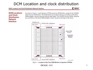
Clock Distribution using Clock Trees Most common method for distributing clock signals is the clock tree method. Buffers are placed between the clock source and along the clock paths as they branch out towards the clock loads. Distributed buffers are the primary source of the total clock skew because active device characteristics typically vary more than passive device characteristics. Sachin: MEE Project Defense
Clock Tree of DEC Alpha 21064 In this five stage buffer tree design, one of the intermediate clock tree stages was made into a mesh by strapping metal lines across each of the branches. The mesh structure places the interconnect resistance in parallel, reducing the effective resistance seen by the buffers. This minimizes both the delay through the clock distribution and the total skew within it. Advantages of this strategy are the removal of the skew introduced by the distributed buffers, and the reduced area obtained by eliminating the distributed buffers. Sachin: MEE Project Defense
H - Tree This method aims to produce zero skew clock routing by matching the length of every path from clock source to register load. At each junction the impedance of the interconnect is scaled to minimize reflections. For an H-tree network, each conductor leaving a junction must have twice the impedance of the source conductor. This is accomplished by decreasing the interconnect width of each successive level. Sachin: MEE Project Defense
Challenges • Clock network is non-uniform. • Increasing process and device variations adds to clock skews. • Requires chain of clock buffers to deliver ultimate driving capability. • Buffers subject to power supply noise and contribute to Jitter. • Jitter and skew combined represent about 18% of cycle time currently, and that results in indirect energy waste. • For a fixed cycle time budget, any increase in jitter and skew reduces the time left for the logic. • To compensate and make the circuitry faster, the supply voltage is raised, therefore increasing energy consumption. Sachin: MEE Project Defense
Wireless Clock Distribution • An approximately 20-GHz signal is generated on-chip and applied to an integrated transmitting antenna which is located at one part of the IC. • Clock receivers distributed throughout the IC detect the transmitted signal using integrated antennas, and then amplify and synchronously divide it down to a 2.5-GHz local clock frequency. • These local clock signals are then buffered and distributed to adjacent circuitry. • Benefits • Reduces latency in clock tree which helps reduce the skew • Eliminates frequency dispersion problem that may ultimately limit the maximum clock frequency Sachin: MEE Project Defense
Intra and Inter Chip Wireless Clock B. Floyd, C.M. Hung, and K. O. Kenneth, “Intra-Chip Wireless Interconnect for Clock Distribution Implemented With Integrated Antennas, Receivers, and Transmitters,” IEEE Jour. Solid-State Circuits, vol. 37, pp. 543–552, 2002. Sachin: MEE Project Defense
Clock Transmitter and Receiver B. Floyd, C.M. Hung, and K. O. Kenneth, “Intra-Chip Wireless Interconnect for Clock Distribution Implemented With Integrated Antennas, Receivers, and Transmitters,” IEEE Jour. Solid-State Circuits, vol. 37, pp. 543–552, 2002. Sachin: MEE Project Defense
Comparison of Power Assumptions • System voltage and frequency are assumed to be equal. • An equal capacitive load representing local clock generators or distribution system is assumed for each type of global distribution system. Under these assumptions, the power dissipation can be converted to capacitances and these can be used to compare the power dissipation of different global distribution systems. Total Global Capacitance = CG + CW + CL where, CG- Equivalent capacitance of the highest level network CW - Capacitance of the interconnecting wires CL - Load capacitance or input capacitance of the local clock generators Sachin: MEE Project Defense
Global Capacitive Loading Grid System based on DEC 21264 H – Tree System based on IBM S/390 B. A. Floyd and K. O. Kenneth, “The Projected Power Consumption of a Wireless Clock Distribution System and Comparison to Conventional Distribution Systems,” in Proc. IITC, 1999. Sachin: MEE Project Defense
Other Benefits • Signal propagation occurs at speed of light, shortening the global interconnect delay without requiring integrated optical components. • Global interconnect wires are eliminated freeing up space. • Inter-chip clock distribution system can provide global clock signals with a small skew to an area much greater than the projected IC size. • Dispersive effects are minimized since a monotone global clock signal is transmitted. • More uniformly distributed power load equalizing temperature gradients across the chip. • By adjusting the division ratio in the receiver, higher frequency local clock signals can be obtained. Sachin: MEE Project Defense
Future Work • Wireless Clock Distribution • External power amplifiers (PAs) are used to increase the power level of the transmitted clock signal. External PAs increases the system complexity and increases the cost. They should be replaced by an on-chip PA. • The local clock signal frequency is limited by the operating frequency of clock transmitter and receiver. There is much room for increasing the clock frequency. With the increase of clock frequency, the on-chip receiving antenna size can be reduced, which will reduce the on-chip receiving antenna area, a major problem in the system. Sachin: MEE Project Defense
Optical Clock Distribution Optical interconnects for clock distribution were first studied by Goodman et al. Interconnect delays will be the limiting factor for performance in future MOS circuits and suggest moving to optical and electro-optic technologies. Advantages in moving to Photonics • Freedom from capacitive loading effects which allows greater fan-in and fan-out. • Immunity to mutual interference effects. • Lack of planar constraints resulting in reduced cross-coupling for criss-crossing waveguides. • Re-configurability of free space focused interconnects. • Possibility of direct injection of optical signals into electronic devices without the need for optical to electrical conversion. Sachin: MEE Project Defense
Types of Optical Clocking • Index-based with waveguides • Index-based with fiber optics • Unfocused free space interconnect • Focused free space interconnect Sachin: MEE Project Defense
Index-based with Fiber Optics J. W. Goodman, F. Leonberger, S.-Y. Kung, and R. A. Athale, "Optical Interconnections for VLSI Systems," Proceedings of the IEEE, vol. 72, no. 7, pp. 850-866, July 1984. Sachin: MEE Project Defense
Index-based with Fiber Optics • A bundle of fibers is fused together at one end, yielding a core into which light from the modulated optical source must be coupled. • Light coupled in at the fused end is split as the cores separate, and transmitted to the ends of each of the fibers in the bundle. • Each fiber end must now be carefully located over an optical detector that will convert the optical clock to an electrical one. • Difficulties associated with the fiber-optic approach stem from the alignment requirements for the fibers and detectors, and from the uniformity requirements for the fused-fiber splitter. • Fibers cannot be allowed to bend too much, for bends will cause radiation losses that may become severe. • This interconnect technology will occupy a three-dimensional volume which is a major disadvantage. Sachin: MEE Project Defense
Index-based with waveguides Sachin: MEE Project Defense
Index-based with waveguides • Optical signals must be coupled into each of the separate guides. • Single or multiple sources. • Light must be coupled out of each of the straight waveguides at several sites along its length, with a detector converting the optical signal to electronic form at each such site. • Careful alignment of the sources or fibers with the integrated waveguides is required. Sachin: MEE Project Defense
Unfocused free space interconnect Sachin: MEE Project Defense
Unfocused free space interconnect • Modulated optical source is situated at a focal point of a lens that resides above the chip. • Signal transmitted by that source is collimated by the lens, and illuminates the entire chip at normal incidence. • Detectors integrated in the chip receive the optical signals with identical delays, due to the particular location of the source at the focal point of the lens. • In principle there is no clock skew whatever associated with such a broadcast system. • The system is very inefficient, for only a small fraction of the optical energy falls on the photosensitive areas of the detectors, and the rest is wasted. • Optical energy falling on areas of the chip where it is not wanted may induce stray electronic signals that interfere with the proper operation of the chip. Sachin: MEE Project Defense
Focused free space interconnect Sachin: MEE Project Defense
Focused free space interconnect • The optical source is actually imaged by an optical element onto a multitude of detection sites simultaneously. • The required optical element can be realized by means of a hologram, to generate focused grating components at the desired locations. • The efficiency of such a scheme can obviously exceed that of the unfocused case, provided the holographic optical elements have suitable efficiency. • Chief disadvantage of the focused interconnect technique is the very high degree of alignment precision that must be established and maintained to assure that the focused spots are striking the appropriate places on the chip. Sachin: MEE Project Defense
Optical Clock Distribution System Sachin: MEE Project Defense
Optical Clock Distribution System • The optical clock source is optically coupled to the distribution network, which is optoelectronically coupled to an optical detector that converts incident optical energy into current pulses. • The recovery and signal condition stage then amplifies the current pulses to generate corresponding rail-to-rail electrical clock signal for local distribution. • Clock signal is distributed to the entire chip by dividing the chip into clock domains and placing a clock recovery resource or transimpedance amplifier (TIA) station in each domain. Sachin: MEE Project Defense
Optical H-Tree with TIA A Trans-impedance amplifier (TIA) is used to convert, amplify and condition the photo current to generate rail-to-rail electrical clock signal. Sachin: MEE Project Defense
Comparison of Power • Low-power vertical cavity surface emitting laser (VCSEL) is used as an off-chip photonic source. • The number and placement of the receivers in optical clock system is equivalent to the number and placement of the output nodes in the electrical H-tree. • At the receivers, the high speed optical signal is converted to an electrical signal and subsequently distributed by the local electrical networks. • The number of Optical to Electrical converters is a particularly crucial parameter in the overall system since optoelectronic interface circuits at these points are of-course necessary and consume power. • Comparison made on 70nm technology. Sachin: MEE Project Defense
Experimental Setup G. Tosik, Z. Lisik, and F. Gaffiot, “Optical Interconnections in Future VLSI Systems,” Journal of Telecommunications and Information Technology, pp. 105–108, 2007. Sachin: MEE Project Defense
Result • Initially power consumed by Optical clock is less than Electrical system. • At 8172 nodes, power consumed by Optical is more than Electrical. G. Tosik, Z. Lisik, and F. Gaffiot, “Optical Interconnections in future VLSI systems,” Journal of Telecommunications and Information Technology, pp. 105–108, 2007. Sachin: MEE Project Defense
Variation of Clock Skew with Temperature • With the growth of chip temperature, the refractive index of waveguide core increases thus reducing the speed of clock signal. • The calculation has been performed for the chip structure where the temperature of one part is lower (350 K), while that of the other part is higher (400 K) Sachin: MEE Project Defense
Result • Clock skew of a 64-output-node optical H-tree compared to the clock period as a function of technology. • For the 32 nm technology node and below the clock skew is higher than 10% of the clock period. This will result in a serious system failure. Sachin: MEE Project Defense
Benefits • Has the potential to continue to scale with future generations of silicon integrated circuits. • Ability to send signals across in third dimension. Sachin: MEE Project Defense
Future Work • Optical Clock Distribution • Optoelectronic devices require continued development to meet the yield, tolerance, and drive voltage requirements for practical systems with future generations of silicon CMOS. • Research is needed in circuits that, i) avoid issues such as crosstalk and susceptibility to digital noise, ii) have appropriately low power dissipation and latency, and iii) are tolerant to process variations. • The technology for integrating optoelectronics with silicon integrated circuits is still at an early stage. • Optics can likely enable kinds of architectures that are not well suited to electrical interconnect systems and can likely also allow continued use of current architectures that otherwise would have to be abandoned in the future because of the limitations of wired interconnects. Sachin: MEE Project Defense
References • “The International Technology Roadmap for Semiconductors,” 2005. Semiconductor Industries Association, San Jose, California. • B. Floyd, C.M. Hung, and K. O. Kenneth, “Intra-Chip Wireless Interconnect for Clock Distribution Implemented With Integrated Antennas, Receivers, and Transmitters,” IEEE Jour. Solid-State Circuits, vol. 37, pp. 543–552, 2002. • B. A. Floyd and K. O. Kenneth, “The Projected Power Consumption of a Wireless Clock Distribution System and Comparison to Conventional Distribution Systems,” in Proc. IITC, 1999. • E. Friedman, Clock Distribution Networks in VLSI Circuits and Systems. New York: IEEE Press, 1995. • M. Horowitz, “Clocking Strategies in High Performance Processors,” in Proceedings of the IEEE Symposium on VLSI Circuits, June 1992, pp. 50–53. • P. J. Restle and A. Deutsch, “Designing the Best Clock Distribution Network,” in Proc. Symp. VLSI Circuits, 1998, pp. 2–5. • G. Tosik, Z. Lisik, and F. Gaffiot, “Optical Interconnections in future VLSI systems,” Journal of Telecommunications and Information Technology, pp. 105–108, 2007. • J. W. Goodman, F. Leonberger, S.-Y. Kung, and R. A. Athale, "Optical Interconnections for VLSI Systems," Proceedings of the IEEE, vol. 72, no. 7, pp. 850-866, July 1984. Sachin: MEE Project Defense