Download
1 / 18
180 likes | 336 Views
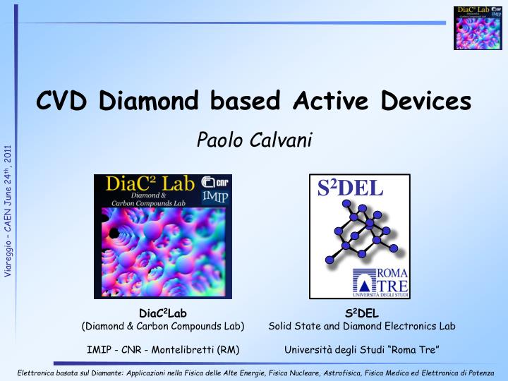
CVD Diamond based Active Devices. Paolo Calvani. S 2 DEL. DiaC 2 Lab (Diamond & Carbon Compounds Lab) IMIP - CNR - Montelibretti (RM). S 2 DEL Solid State and Diamond Electronics Lab Università degli Studi “Roma Tre”. Daniele M. Trucchi Paolo Calvani Alessandro Bellucci Emilia Cappelli

E N D
CVD Diamond based Active Devices Paolo Calvani S2DEL DiaC2Lab (Diamond & Carbon Compounds Lab) IMIP - CNR - Montelibretti (RM) S2DEL Solid State and Diamond Electronics Lab Università degli Studi “Roma Tre”
Daniele M. Trucchi Paolo Calvani Alessandro Bellucci Emilia Cappelli Stefano Orlando
CNR-IMIP: Know-How & Projects 1989-1995 Study of Nucleation and Growth Mechanisms of CVD Diamond 1995-1999 CVD Diamond protective coatings of cutting tools Coordination of MURST-CNR 5% Project 2003-2006 Development of high-tech materials and ceramic coatings ENEA-MIUR “PROMOMAT” Strategic Project 1999-2001 Secondary electron emission amplifiers for scanning electron microscopy MADESS II Applied Research Project 2000-2002 VUV & DUV Radiation Detectors in collaboration with S2DEL – Univ. Roma Tre ASI ARS1/R07/01 Aerospace Project 2001-2005 Poly-Diamond Radiation Dosimeters for Radiation Therapy Coordination of European Project “DIAMOND” G5RD-CT01-00603 2003-2007 Nanostructured Carbon and graphene Structures for Opto-Electronic applications FIRB Project “Micro & Nanocarbon” & FISR Project “High Density Memories” 2008-2010 Systems for direct nuclear-to-electric energy conversion Coordination of CNR-RSTL “ECO-Diamond” Project 2008-today Development of Single-Crystal Diamond dosimeters in collaboration with S2DEL - Univ. Roma Tre 2010-2013 Thermionic-thermoelectric conversion module for solar concentrated systems E2PHEST2US Project Mechanical Applications Electronic Applications
~ Secondary Electron Emission Characterization Setup Vacuum & Temperature Electronic Characterization (VTEC) (10-9 Torr, T=77-1200 K) for Thermionic Emission Raman & IR SEM & EDS AFM X-Ray Photoconductivity Setup Spectral (UV-Vis-NIR) Photoconductivity Setup MW-CVD for surface hydrogen termination RF Sputtering for deposition of metals Ti, Al, Cr, … Four-Point Probe under vacuum, T=25-400 °C CNR-IMIP: Facilities Characterization of Device Performance Characterization of Chemical-Physical Properties Material Production Technological Processes for Device Fabrication Spectroscopy Hot Filament CVD for diamond film deposition Microwave CVD for diamond (doped) film deposition Spectral Photometry Microscopy Pulsed laser (Excimer & Nd:YAG) ablation for (nanostructured) thin-film deposition of carbon, carbides, refractory metals Seebeck Effect Measurement System for Thermoelectric Characterization
Diamond Electronic Properties • High Frequency – High Power Field Effect Transistors • UV Power Switches • Renewable Energies Conversion Stages
High Frequency – High Power Field Effect Transistors Plasma assisted Hydrogen termination of CVD Diamond induces p-type conductive channel Fabricated by S2DEL and IFN-CNR Evolution of the band bending, activated by air exposure, during the electron transfer process at the interface between diamond and water layer[b]: density-of-states (DOS) is changing from 3D to 2D: 2DHG S2DEL
RF Power Characterization by Politecnico di Torino CLASS A @ 2GHz Pout=0.2 W/mm Gain=8 dB PAE=21.3% Pout @ 1GHz ~ 0.8 W/mm[a] Best result for Polycrystalline Diamond LG=200nm, WG=50um VDS=-14 V, VGS=-0.3 V fMAX = 15.2 GHz ft = 6.2 GHz S2DEL MaximumVDS applied=80 V Eapplied= 2 MV/cm Channel conductance is always positive. No self heating effects!
Polycrystalline Diamond PolyD4 by Russian Academy of Sciences Single Crystal Diamond P7MS by Russian Academy of Sciences Wg=50 μm -20 dB/dec. WG=25 μm fMAX =26.3 GHz fMAX = 23.7 GHz Gain = 15 dB@ 1 GHz fT = 6.9 GHz fT = 13.2 GHz S2DEL Gain = 22 dB @ 1 GHz LG=0.2 μm VGS=-0.2 V, VDS=-10 V Eapplied= 0.5 MV/cm RF Small Signal Characterization in collaboration with by Tor Vergata University
Polycrystalline Diamond PolyD4 by Russian Academy of Sciences Lg=0.2 μm, Wg=25 μm VGS=0.0 V, VDS=-35 V -20 dB/dec. fMAX = 35 GHz Gain = 16 dB @1GHz fT = 10 GHz S2DEL Eapplied= 1.75 MV/cm
Lecroy WavePro 960 2 GHz 16Gs/s digital oscilloscope Picosecond 5550B 18 GHz Bias tee Neweks PSX 100 excimer laser Filled with ArF gas mixture VDS DUT Si diode (for trigger) =193 nm 50 Oscilloscope input resistance x GPIB Laser pulse shape recorded by vacuum phototube VGS (Keithley 617) UV POWER SWITCHES S2DEL
12/23 Source Drain G UV generated carriers diamond VDS=-9.6 V VGS=-3.4 V
13/23 Source Drain G UV generated carriers diamond
Renewable Energies Conversion Stage EU Project E2PHEST2US’ • Duration: 3 years (Jan 2010 - Jan 2013) • Total Project Cost: 2.68 M€ • Total EU Funding: 1.98 M€ • Partners: • CNR (Italy, Scientific Coordination) • CRR (Italy, Management Coordination) • SHAP (Italy) • Tel Aviv University (Israel) • Tubitak (Turkey) • Prysmian (Multinational Industry) • Maya (San Marino) *For details, http://www.ephestus.eu
T z EU Project E2PHEST2US’ Thermionic Stage Load Radiation Absorber Collector Thermoelectric Stage Load Rload Rload p n Under Vacuum Concentrated Solar Radiation (400 – 1000 suns) p n p n Thermionic Emitter Inter-electrode Space (<1 mm) • Development of: • A radiation absorber made of ceramic materials able to work stably at high temperature (700 - 1000 °C) • A thermionic conversion stage with CVD diamond as the active material • A thermoelectric conversion stage constituted by high Seebeck coefficient materials • Maximum theoretical efficiency ≈ 30% Final Thermal Stage TR (700-1000 °C) Thermoelectric Stage TE TC (250-400 °C) TTE TAmb *For details, http://www.ephestus.eu
CVD Diamond based Active Devices Thanks for the attention S2DEL DiaC2Lab (Diamond & Carbon Compounds Lab) IMIP - CNR - Montelibretti (RM) S2DEL Solid State and Diamond Electronics Lab Università degli Studi “Roma Tre”
Alternative Technology in Concentrating Systems • Multi-junction Photovoltaic Cells • Thermodynamic Conversion by Heat Engines (Stirling, Rankine) • Nominal Conversion Efficiency of 30% • Compactness • No mechanical parts in movement • Highly Expensive • Mandatory Need of Cooling (Conversion Efficiency Exponentially Decreases with Temperature) • Illumination Local Inhomogeneities Causes Output Bottlenecks • Production Dependent on Semiconductor Industry (Few Large-Scale World Suppliers) • Nominal Conversion Efficiency of 35% at High Temperatures (> 600 °C) • Not Compact System • Mechanical Parts in Movement (Degradation with Operative Time) • Economically Reasonable for Large Plants (> 10 kWe)