Download
1 / 13
130 likes | 194 Views
Computer Systems Architecture A networking Approach Chapter 12 Introduction The Memory Hierarchy. CS 147 Nathaniel Gilbert. Levels of Performance – You Get What You Pay For. Recall: Dynamic Random Access Memory (DRAM) Capacitors to store state (0 or 1) Periodically refreshed

E N D
Computer Systems ArchitectureA networking ApproachChapter 12 IntroductionThe Memory Hierarchy CS 147 Nathaniel Gilbert
Levels of Performance – You Get What You Pay For Recall: • Dynamic Random Access Memory (DRAM) • Capacitors to store state (0 or 1) • Periodically refreshed • Relatively cheap • Static Random Access Memory (SRAM) • Transistors to store state • Doesn’t need to be refreshed, faster, and uses less power than DRAM • More expensive than DRAM
Levels of Performance cont. Currently, one Pound is about 2 US Dollars. R = removable media
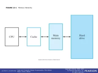
Levels of Performance cont. Storage Hierarchy – fastest CPU registers at top, slowest tape drives at bottom Pre-fetching – Data transferred between layers is usually bigger than requested. This is to anticipate using the extra blocks of data.
Localization of Access – exploiting repetition • Computers tend to access the same locality of memory. • This is partly due to the programmer organizing data in clusters along with the compiler attempting to organize code efficiently. • This localization can be exploited in memory hierarchy.
Localization of Access cont. • Exploiting localization of memory access • Keep related data in smaller groups (try not to store all input and output to a single array when reading from/writing to disk) • Only the portion of data the CPU is using should be loaded into faster memory.
Localization of Access cont. The following code was used by the author to demonstrate cache action (exploiting localization of memory access)
Localization of Access cont. • On a sun workstation (200 MHz CPU, 256 Mbyte main memory, 256 kbyte cache, 4 Gbyte local hard drive), the output was: (Time is system clock ticks)
Localization of Access cont. • The reason for the doubling of time is the movement of data up and down the data hierarchy. • The array is sent to higher memory in blocks because the 256 kbytes of cache memory cannot hold the whole object.
Instruction and Data Caches – Matching Memory to CPU Speed • A 2 GHz Pentium CPU accesses program memory an average off 0.5 ns just for fetching instructions • DDO DRAM responds within 10 ns. If the CPU only used DRAM, it would result in 20x loss in speed • This is where using SRAM (cache) comes into play • Downfall of cache: • Misses (if the desired code is not in the memory segment) may take longer because the memory has to be reloaded • Negative cache – (depending on architecture) where negative results (failures) are stored
Instruction and Data Caches cont. • Cache is built from SRAM chips, and ideally are made to match the system clock speed of a CPU • The Cache Controller Unit (CCU) and cache memory, are inserted between the CPU and the main memory. • Level 1 and Level 2 cache are different by placement. • Level 1 is on the CPU chip. • Level 2 was generally located off the CPU chip and was slowed down by the system bus. Intel successfully integrated a 128 kbyte L2 cache memory onto the CPU and continues to offer integrated chips.
Instruction and Data Caches cont. • Generic System Architecture • Level 1 is the microprocessor with three forms of cache: • D-cache – (Data) Fast buffer containing application data • I-cache – (Instruction) Speed up executable instruction • TLB – (Translation Lookaside Buffer) Stores a map of translated virtual page addresses • Level 2 is Unified cache • Memory – DRAM • CPU and Register file reside in Level 1 • Register file – Small amount of memory closest to CPU where data is manipulated