Download
1 / 16
160 likes | 316 Views
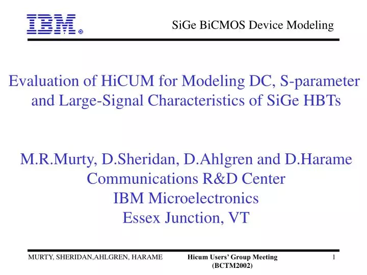
Evaluation of HiCUM for Modeling DC, S-parameter and Large-Signal Characteristics of SiGe HBTs M.R.Murty, D.Sheridan, D.Ahlgren and D.Harame Communications R&D Center IBM Microelectronics Essex Junction, VT. Model Extraction Methodology and Technology Details.

E N D
Evaluation of HiCUM for Modeling DC, S-parameter and Large-Signal Characteristics of SiGe HBTs M.R.Murty, D.Sheridan, D.Ahlgren and D.Harame Communications R&D Center IBM Microelectronics Essex Junction, VT Hicum Users’ Group Meeting (BCTM2002)
Model Extraction Methodology and Technology Details • Transistor Structures used for Parameter Extraction: • (0.32, 0.48, 0.64, 0.96) m x 8.4 m with a CBEBC layout • Scaling by TRADICA and Models extracted on structures with a CBE layout • Simulations and Optimizations done in ADS2001 & ADS2002. • Technology Details:High-Speed and High-Breakdown Versions with ~47GHz and 27 GHz fT and BVCEO of ~3.5V and 5.5V. Hicum Users’ Group Meeting (BCTM2002)
Parameter Extraction • Base Resistance Ring-Emitter Structures (several W’s and 2 L’s) • Emitter Resistance Modified Open-Collector Method • Collector Resistance Test Structures • Capacitances Cold S-Params + Large area monitors • Avalanche Parameters: Ib vs Vbc Characteristics • Current Parameters Gummels and Output Curves • Transit Time Parameters: Test Transistors (several W’s and one long L) Hicum Users’ Group Meeting (BCTM2002)
Ic & Ib (A) Gummel Curves and Forward Gain -0.32 um x 16.8 um, HB device Hicum Users’ Group Meeting (BCTM2002)
Output Curves -0.32 um x 16.8 um, HB device Hicum Users’ Group Meeting (BCTM2002)
S-Parameter Results • Bias Points: Vbe = 0.82 V, 0.90 V, 0.93 V and Vce = 2 V. • (1 below ft peak, one at peak ft and one past ft peak) • Frequency range: 2-40 GHz. • Optimizations were done using Y-parameters (in ADS). • Ft-Ic: Vcb = -0.3, 0, 1.0, 2.0, 3.0 V Hicum Users’ Group Meeting (BCTM2002)
Phase(S11) S11 -0.32 um x 16.8 um, HB device o Vbe = 0.82 V, Vce= 2 V, o Vbe = 0.90 V, Vce= 2 V, o Vbe = 0.93 V, Vce= 2 V, __ Model Hicum Users’ Group Meeting (BCTM2002)
S21 -0.32 um x 16.8 um, HB device o Vbe = 0.82 V, Vce= 2 V, o Vbe = 0.90 V, Vce= 2 V, o Vbe = 0.93 V, Vce= 2 V, __ Model Hicum Users’ Group Meeting (BCTM2002)
S12 -0.32 um x 16.8 um, HB device o Vbe = 0.82 V, Vce= 2 V, o Vbe = 0.90 V, Vce= 2 V, o Vbe = 0.93 V, Vce= 2 V, __ Model Hicum Users’ Group Meeting (BCTM2002)
S22 -0.32 um x 16.8 um, HB device o Vbe = 0.82 V, Vce= 2 V, o Vbe = 0.90 V, Vce= 2 V, o Vbe = 0.93 V, Vce= 2 V, __ Model Hicum Users’ Group Meeting (BCTM2002)
|H21| and MAG/MSG -0.32 um x 16.8 um, HB device o Vbe = 0.82 V, Vce= 2 V, o Vbe = 0.90 V, Vce= 2 V, o Vbe = 0.93 V, Vce= 2 V, __ Model Hicum Users’ Group Meeting (BCTM2002)
|fT vs Ic -0.32 um x 16.8 um, HB device o Measurement __ Model (Vcb = -0.3, 0, 1, 2, 3 V) Hicum Users’ Group Meeting (BCTM2002)
Intermodulation Distortion Results • Measurements done using ATN Load-pull system and Simulations • Using Harmonic Balance • 2-tone Simulations and Intermodulation Distortion with • 50 termination, Sheridan, Murty and others • CMC,April 2001 (PortoRico) & present work • 1-tone Simulations and harmonic Distortion with a 50 termination • Schroter et.al., IEEE TED, 47, pp1529-1535 (2000) • 2-tone Intermodulation Distortion with matched load and source • Murty et.al., (To be published) Hicum Users’ Group Meeting (BCTM2002)
Ic & Ib (mA) Pout, IM3, IM5 (dBm) |Pout, IM3, IM5, Ic and Ib -0.32 um x 16.8 um, HB device __ Hicum o Vbe = 0.9109 V, Vce= 2 V,f= 900 MHz, =0.1 MHz __ Hicum simulations using Harmonic Balance Hicum Users’ Group Meeting (BCTM2002)
Conclusions • Hicum Model is developed for a SiGe process and good fits • demonstrated for DC, S-parameter and Large-signal characteristics. • The simulations were done in ADS2001/02 and the model • implementation is found to be robust. • (at least at the device level) Hicum Users’ Group Meeting (BCTM2002)
ACKNOWLEDGEMENTS Thanks to M.Schroter, K.Newton, W.Ansley for many useful discussions Hicum Users’ Group Meeting (BCTM2002)