Download
1 / 1
10 likes | 225 Views
Basic Idea: Create highly-pure, highly-ordered bound organo-silicon hybrids Molecules bound so intimately that electron waves pass easily between components Yielding: 1) Precise charge transfer in to and out of Si surfaces 2) Conduction based on quantum mechanical resonance

E N D
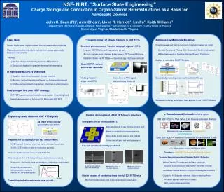
Basic Idea: Create highly-pure, highly-ordered bound organo-silicon hybrids Molecules bound so intimately that electron waves pass easily between components Yielding: 1) Precise charge transfer in to and out of Si surfaces 2) Conduction based on quantum mechanical resonance In nanoscale MOSFETs this could: Supplant conventional trace donor/acceptor charge creation Minimize ionized impurity scattering => Enhanced transport Enable devices based on quantum interference phenomenon Three pronged investigation strategy: First principles modeling Studies of trap-influenced transport in CNT & graphene surrogates Development of full organo-Si MOSFET device structure Multiscale Modeling of Trap Modified Transport: Coupling weak and strong quantum correlation (wires vs. dots): Density Functional Theory (Si) / Extended Hückel (molecules) Within framework of Non-Equilibrium Green's Functions Applied to Random Telegraph Signals (RTS) of molecules on FETs: Could differentiate between molecules and alternate binding states: • Effect of Traps on CNT and Graphene Transport: • Basic studies + “concurrent engineering” of experimental techniques and modeling tools for later use with full SOI MOSFET device • Electron beam induced traps in CNT and graphene FETs: • RTS successfully modeled, including multi-trap interactions • Inter vs. intra layer transport in Graphene: • Despite common 2D idealizations, real data likely to include both! • Raman highly sensitive to layer edges => Decorate with metals • Colloidal Ag decoration Raman of Raman of Ag edge • of graphene edges normal HOPG decorated HOPG • Signature should facilitate deconvolution of transport modes NSF- NIRT: "Surface State Engineering"Charge Storage and Conduction in Organo-Silicon Heterostructures as a Basis for Nanoscale DevicesJohn C. Bean (PI)1, Avik Ghosh1, Lloyd R. Harriott1, Lin Pu2, Keith Williams31Department of Electrical and Computer Engineering, 2Department of Chemistry, 3Department of PhysicsUniversity of Virginia, Charlottesville Virginia Outreach: Continuing Development of “Hands-on Intro to Nano” Class Begun under 2005 NSF NUE grant Complete class website (with visitors from over 1000 schools): www.virlab.virginia.edu/Nanoscience_class/Nanoscience_class.htm Cited in 2009 Award of IEEE Undergraduate Teaching Medal to PI Plus ongoing summer Nano classes for K-12 science teachers Recent Project Publications: Reversal of current blockade in nanotube-based field effect transistors through multiple trap correlations, J. Chan et al., Phys. Rev. B80, 033402 (2009) Controlling transistor threshold voltages using molecular dipoles, S. Vasudevan et al., J. Appl. Phys.105, 093703 (2009) Modeling electrostatic and quantum detection of molecules, S. Vasudevan et al., IEEE-Sensors Journal 8, 6 (2008) Plus In-Press / In-Preparation: Quantum Transport through Metal-Molecule-Semiconductor heterostructures: the role of interfacial charges and barriers, A Bahuguna et al. Coupling nano and microscale transport for electronic read-out of quantum dot dynamics, S. Vasudevan et al. Single Molecule Characterization using Random Telegraph Signals, S. Vasudevan et al. Microscopic model for trap-generated noise in nano-devices, S. Vasudevan et al. (Engineering of Molecular Surface States on Si continued): Fine-tuned with fluorine induced dipoles vs. quadrupoles: Or via dilution of surface-state-inducing molecules with passivating molecules Dipole induced surface band bending actually more intense in diluted layers: Evidence that polar organics partially depolarize if in immediate proximity Task 4: Fabrication of back-gated SOI MOSFET device structure Goal: Assess channel modification via phenomena such as RTS signals Pursuing both micron and deep sub-micron channel width device designs Former: Easier to fabricate / Latter: More subtle surface state information Component processes for both designs essentially complete: Design Pads Channel Side-gates Engineering Molecular Surface States on Silicon: Task 1: Achieve dense high-quality organic attachment to Si Achieved via UV-enhanced UHV vacuum hydrosilylation (e.g. alkyne => alkene + attachment): Task 2: Identify organics capable of passivating Si surfaces Hydrosilylated acetylene proved very effective as verified by pulsed photoconductivity measurement of near surface Si minority carrier lifetimes Task 3: Develop palette of organic surface state inducers Surface dipoles: Surface charge transfer: First achieved with variants of phenylacetylene: