Download
1 / 46
460 likes | 518 Views
This text discusses the allocation of space for variables in memory, including the global data section, run-time stack, and activation record. It also explains interrupt handling and programmable logic arrays (PLAs).

E N D
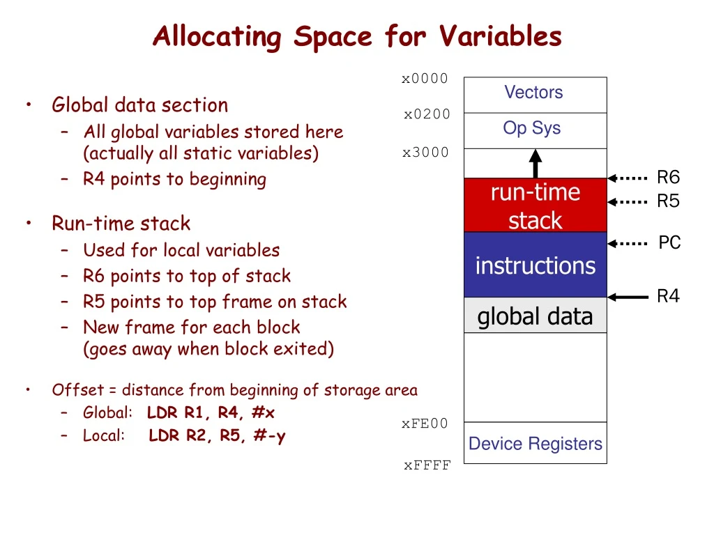
Allocating Space for Variables x0000 Vectors x0200 Op Sys • Global data section • All global variables stored here(actually all static variables) • R4 points to beginning • Run-time stack • Used for local variables • R6 points to top of stack • R5 points to top frame on stack • New frame for each block(goes away when block exited) • Offset = distance from beginning of storage area • Global: LDR R1, R4, #x • Local: LDR R2, R5, #-y x3000 R6 run-time stack R5 PC instructions R4 global data xFE00 Device Registers xFFFF
Activation Record or Context Frame Format R6 Function stacked stuff …….. …….. Local Variables Caller’s Frame Pointer (R5) Caller’s Return PC (R7) Function Return Value Function Pass Value n …….. Function Pass Value 1 R5
Interrupts: • Programmer Action: Enable Interrupts by setting “intr enable” bit in Device Status Reg • Enabling Mechanism for device: When device wants service, and its enable bit is set (The I/O device has the right to request service), and its priority is higher than the priority of the presently running program, and execution of an instruction is complete, then The processor initiates the interrupt • Process to service the interrupt: The Processor saves the “state” of the program (has to be able to return) The Processor goes into Privileged Mode (PSR bit 15 cleared) Priority level is set (established by the interrupting device) The (USP), (R6) USP.saved register (UserStackPointer.saved) The (SSP.saved) R6 (SupervisorStackPointer) The (PC) and the (PSR) are PUSHED onto the Supervisor Stack The contents of the other registers are not saved. Why? The CC’s are cleared • The Processor Loads the PC from the Interrupt vector (vectors in 0100:01FF) • Interrupt Service Routine is executed Ends with an RTI • Program returns from Service routine The stored user PSR (POP into PSR), PC (POP into PC), (R6)SSP.saved, (USP.savedR6), and the next instruction fetched
Hardware Foundation Logic Gates Logic Chips Combinational Logic Timing Sequential Logic Flip Flops Registers State Machines Memory
CMOS Device - Inverter 3-5 volts p channel device CMOS Inverter n channel device
CMOS NOR Gate NOR Gate
CMOS OR Gate OR Gate
CMOS AND Gate AND Gate
2-to-1 MUX MUX Circuit Case: S=0 MUX Symbol
4-to-1 MUX Symbol Logic
D 0 8 to 1 MUX D 1 D 2 D 3 F D 4 D 5 D 6 D 7 A A B B C C A B C
Standard Symbols for Multiplexers 8 to 1 Vector(2) of 4 to 1 Vector(4) of 2 to 1
4 Bit Full Adder 1 bit adder 4 bit adder How many gate delays will it take before all of the outputs are correct?
Logical Completeness • Can implement ANY truth table with AND, OR, NOT. 1. AND combinations that yield a "1" in the truth table. 2. OR the resultsof the AND gates. • ALSO: • Can implement ANY truth table with ONLY NANDS. • Can implement ANY truth table with ONLY NORS.
Programmable Logic Arrays (PLAs) • Any combinational logic function can be realized as a sum of products. • Idea: Build a large AND-OR array with lots of inputs and product terms, and programmable connections. • n inputs • AND gates have 2n inputs -- true and complement of each variable. • m outputs, driven by large OR gates • Each AND gate is programmably connected to each output’s OR gate. • p AND gates (p<<2n) • designation is n x m, p ANDs
Example: 4x3 PLA, 6 product terms--- X locates a fuse that can disconnect a line
Example: PAL16L8 Programmable Array Logic (PALs) • How beneficial is product sharing? • Not enough to justify the extra fuse array • PALs ==> fixed OR array • Each AND gate is permanently connected to a certain OR gate.
10 primary inputs • 8 outputs, with 7 ANDs per output • 1 AND for 3-state enable • 6 outputs available as inputs • more inputs, at expense of outputs • two-pass logic, helper terms • Note inversion on outputs • output is complement of sum-of-products • newer PALs have selectable inversion
GAL16V8C provides optional inversion via XOR gate close-up on next slide -->
Designing with PLAs • Compare number of inputs and outputs of the problem with available resources in the PAL • Write equations for each output using programming language like ABEL (Xilinx)
Alternative Logic “Family” Choices • Totempole: High or Low output level (Most Common) Line always at a 1 level or 0 level • Tristate: High, Low, or Open (Good for BUS application) Like Totempole, but has third state – open state • Open Collector, Open Drain, Wired-OR:(Older alternative to Tristate – still used, but more susceptible to noise) Line is nominally at a 1 level or 0 level – line is “pulled” to non-nominal level. Outputs of and gates can be connected directed together to create an “OR condition. • Differential:(Used for driving signals a distance. Good noise immunity) Uses a pair of lines – the “level” is the difference of signals on the two lines.
Combinational vs. Sequential Circuits • Combinational Circuit • always gives the same output for a given set of inputs • example: adder always generates sum and carry,regardless of previous inputs • Sequential Circuit • has memory - “stores” information, • output depends on stored information (state) plus input • so a given input might produce different outputs,depending on the stored information • example: ticket counter • advances when you push the button • output depends on previous state • useful for building “memory” elements and “state machines”
Basic SR Flip Flop Nor Gates: S R | Qn+1 0 0 | Qn 0 1 | 0 1 0 | 1 1 1 | Indeterminate a 1 on S or R sets/resets the FF Nand Gates: S R | Qn+1 0 0 | Indeterminate 0 1 | 1 1 0 | 0 1 1 | Qn a 0 on S or R sets/resets the FF
Clocked SR Flip Flop S R | Qn+1 0 0 | Qn 0 1 | 0 1 0 | 1 1 1 | Indeterminate S, R are nominally 0, a 1 on S or R will set/reset the FF AFTER the Clock Pulse
D Flip Flop (D Latch) D | Qn+1 0 | 0 1 | 1
Master Slave Flip Flop Master sets on rising edge of CP, Slave sets on falling edge of CP. (or visa versa depending on the particular Master Slave)
Toggle Flip Flop T | Qn+1 0 | Qn 1 | not Qn Toggles on CP when T =1
JK Flip Flop J K | Qn+1 0 0 | Qn 0 1 | 0 1 0 | 1 1 1 | not Qn
JK as a Universal Flip Flop JK as an SR – use set and pre inputs JK as a Toggle – connect J and K JK as a D – connect NOT J to K
Register • A register stores a multi-bit (vector) value. • We use a collection of D-latches, all controlled by a common write enable pulse, call it WE. • When the write enable WE=1, the n-bit value D is written to register.
More Memory Details Two basic kinds of RAM (Random Access Memory) • Static RAM (SRAM) • fast, maintains data as long as power applied • Dynamic RAM (DRAM) • slower but denser, bit storage decays – must be periodically refreshed. Refreshing interferes with regularity of execution of instruction stream. Also, non-volatile memories: ROM, PROM, flash, …
TCSS372A - HW1 (due October 7) 1) Memory Map & Activation Records: Show the memory map during execution of the following program at point 1 , and the stack at points 1 through point 7. int main () { int a = 23; int b = 14; ... /* point 1 */ b = Watt(a); /* point 5 */ b = Volta(a,b); ... /* point 7 */ } int Watt(int c); { int w = 5; ... /* point 2 */ w = Volta(w,10); /* point 4 */ ... return w; } int Volta(int q, int r) { int k = 3; int m = 6; ... /* point 3 & point 6 */ return k+m; }
HW 1 2) State System Design: Design a “blinking” traffic sign which exhibits the following behavior: • Repeat the following sequence as long as operate switch is turned on: State 1: No lights on State 2: 1 & 2 on State 3: 1, 2, 3, & 4 on State 4: 1, 2, 3, 4, & 5 on - The system is in state 1 when the operate switch is off 3 4 1 5 2 DANGERMOVERIGHT