Download
1 / 105
1.13k likes | 1.51k Views
Semiconductor Theory and Devices. 11.1 Band Theory of Solids 11.2 Semiconductor Theory 11.3 Semiconductor Devices 11.4 Nanotechnology.

E N D
Semiconductor Theory and Devices • 11.1 Band Theory of Solids • 11.2 Semiconductor Theory • 11.3 Semiconductor Devices • 11.4 Nanotechnology It is evident that many years of research by a great many people, both before and after the discovery of the transistor effect, has been required to bring our knowledge of semiconductors to its present development. We were fortunate to be involved at a particularly opportune time and to add another small step in the control of Nature for the benefit of mankind. - John Bardeen, 1956 Nobel lecture
Categories of Solids • There are three categories of solids, based on their conducting properties: • conductors • semiconductors • insulators
0 Electrical Resistivity and Conductivity of Selected Materials at 293 K
Reviewing the previous table reveals that: • The electrical conductivity at room temperature is quite different for each of these three kinds of solids • Metals and alloys have the highest conductivities • followed by semiconductors • and then by insulators
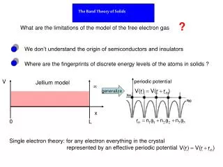
Band Theory of Solids • In order to account for decreasing resistivitywith increasing temperature as well as other properties of semiconductors, a new theory known as the band theory is introduced. • The essential feature of the band theory is that the allowed energy states for electrons are nearly continuous over certain ranges, called energy bands, with forbidden energy gaps between the bands.
Band Theory of Solids • Consider initially the known wave functions of two hydrogen atoms far enough apart so that they do not interact.
Interaction of the wave functions occurs as the atoms get closer: An atom in the symmetric state has a nonzero probability of being halfway between the two atoms, while an electron in the antisymmetric state has a zero probability of being at that location. Band Theory of Solids Symmetric Antisymmetric
In the symmetric case the binding energy is slightly stronger resulting in a lower energy state. Thus there is a splitting of all possible energy levels (1s, 2s, and so on). When more atoms are added (as in a real solid), there is a further splitting of energy levels. With a large number of atoms, the levels are split into nearly continuous energy bands, with each band consisting of a number of closely spaced energy levels. Band Theory of Solids
Sodium 3s1 only one occupied so half full. Empty 3p overlaps with half filled 3s. Easy for valence electrons to jump to higher unfilled states by the presence of a small E field. Above filled states (blue) there are many empty states into which electrons can be excited by even a small electric field. Sodium is a conductor.
Valence band: Band occupied by the outermost electrons Conduction: Lowest band with unoccupied states Conductor: Valence band partially filled (half full) Cu. or Conduction band overlaps the valence band
Resistivity vs. Temperature Figure 11.1: (a) Resistivity versus temperature for a typical conductor. Notice the linear rise in resistivity with increasing temperature at all but very low temperatures. (b) Resistivity versus temperature for a typical conductor at very low temperatures. Notice that the curve flattens and approaches a nonzero resistance as T→ 0. (c) Resistivity versus temperature for a typical semiconductor. The resistivity increases dramatically as T → 0.
Kronig and Penney assumed that an electron experiences an infinite one-dimensional array of finite potential wells. Each potential well models attraction to an atom in the lattice, so the size of the wells must correspond roughly to the lattice spacing. Kronig-Penney Model
Kronig-Penney Model • An effective way to understand the energy gap in semiconductors is to model the interaction between the electrons and the lattice of atoms. • R. de L. Kronig and W. G. Penney developed a useful one-dimensional model of the electron lattice interaction in 1931.
Since the electrons are not free their energies are less than the height V0 of each of the potentials, but the electron is essentially free in the gap 0 < x <a, where it has a wave function of the form where the wave number k is given by the usual relation: Kronig-Penney Model
Tunneling • In the region between a < x < a + b the electron can tunnel through and the wave function loses its oscillatory solution and becomes exponential:
The left-hand side is limited to values between +1 and −1 for all values of K. Plotting this it is observed there exist restricted (shaded) forbidden zones for solutions. Kronig-Penney Model
Matching solutions at the boundary, Kronig and Penney find Here K is another wave number. Kronig-Penney Model
The Forbidden Zones Figure 11.5 (a) Plot of the left side of Equation (11.3) versus ka for κ2ba / 2 = 3π / 2. Allowed energy values must correspond to the values of k for for which the plotted function lies between -1 and +1. Forbidden values are shaded in light blue. (b) The corresponding plot of energy versus ka for κ2ba / 2 = 3π / 2, showing the forbidden energy zones (gaps).
Important differences between the Kronig-Penney model and the single potential well • For an infinite lattice the allowed energies within each band are continuous rather than discrete. In a real crystal the lattice is not infinite, but even if chains are thousands of atoms long, the allowed energies are nearly continuous. • In a real three-dimensional crystal it is appropriate to speak of a wave vector. The allowed ranges for constitute what are referred to in solid state theory as Brillouin zones.
And… • In a real crystal the potential function is more complicated than the Kronig-Penney squares. Thus, the energy gaps are by no means uniform in size. The gap sizes may be changed by the introduction of impurities or imperfections of the lattice. • These facts concerning the energy gaps are of paramount importance in understanding the electronic behavior of semiconductors.
Band Theory and Conductivity • Band theory helps us understand what makes a conductor, insulator, or semiconductor. • Good conductors like copper can be understood using the free electron • It is also possible to make a conductor using a material with its highest band filled, in which case no electron in that band can be considered free. • If this filled band overlaps with the next higher band, however (so that effectively there is no gap between these two bands) then an applied electric field can make an electron from the filled band jump to the higher level. • This allows conduction to take place, although typically with slightly higher resistance than in normal metals. Such materials are known as semimetals.
Valence and Conduction Bands • The band structures of insulators and semiconductors resemble each other qualitatively. Normally there exists in both insulators and semiconductors a filled energy band (referred to as the valence band) separated from the next higher band (referred to as the conduction band) by an energy gap. • If this gap is at least several electron volts, the material is an insulator. It is too difficult for an applied field to overcome that large an energy gap, and thermal excitations lack the energy to promote sufficient numbers of electrons to the conduction band.
Smaller energy gaps create semiconductors • For energy gaps smaller than about 1 electron volt, it is possible for enough electrons to be excited thermally into the conduction band, so that an applied electric field can produce a modest current. The result is a semiconductor.
Temperature and Resistivity • When the temperature is increased from T = 0, more and more atoms are found in excited states. • The increased number of electrons in excited states explains the temperature dependence of the resistivity of semiconductors. Only those electrons that have jumped from the valence band to the conduction band are available to participate in the conduction process in a semiconductor. More and more electrons are found in the conduction band as the temperature is increased, and the resistivity of the semiconductor therefore decreases.
Some Observations • Although it is not possible to use the Fermi-Dirac factor to derive an exact expression for the resistivity of a semiconductor as a function of temperature, some observations follow: • The energy E in the exponential factor makes it clear why the band gap is so crucial. An increase in the band gap by a factor of 10 (say from 1 eV to 10 eV) will, for a given temperature, increase the value of exp(βE) by a factor of exp(9βE). • This generally makes the factor FFD so small that the material has to be an insulator. • Based on this analysis, the resistance of a semiconductor is expected to decrease exponentially with increasing temperature. • This is approximately true—although not exactly, because the function FFD is not a simple exponential, and because the band gap does vary somewhat with temperature.
Clement-Quinnell Equation • A useful empirical expression developed by Clement and Quinnell for the temperature variation of standard carbon resistors is given by where A, B, and K are constants.
Test of the Clement-Quinnell Equation Figure 11.7: (a) An experimental test of the Clement-Quinnell equation, using resistance versus temperature data for four standard carbon resistors. The fit is quite good up to 1 / T≈ 0.6, corresponding to T ≈ 1.6 K. (b) Resistance versus temperature curves for some thermometers used in research. A-B is an Allen-Bradley carbon resistor of the type used to produce the curves in (a). Speer is a carbon resistor, and CG is a carbon-glass resistor. Ge 100 and 1000 are germanium resistors. From G. White, Experimental Techniques in Low Temperature Physics, Oxford: Oxford University Press (1979).
11.2: Semiconductor Theory • At T = 0 we expect all of the atoms in a solid to be in the ground state. The distribution of electrons (fermions) at the various energy levels is governed by the Fermi-Dirac distribution of Equation (9.34): β = (kT)−1 and EF is the Fermi energy.
Holes and Intrinsic Semiconductors • When electrons move into the conduction band, they leave behind vacancies in the valence band. These vacancies are called holes. Because holes represent the absence of negative charges, it is useful to think of them as positive charges. • Whereas the electrons move in a direction opposite to the applied electric field, the holes move in the direction of the electric field. • A semiconductor in which there is a balance between the number of electrons in the conduction band and the number of holes in the valence band is called an intrinsic semiconductor. Examples of intrinsic semiconductors include pure carbon and germanium.
Splitting of 2s and 2p for Carbon , 2s2, 2p2 3s2 3p2 for Silicon 4s24p2 for Germanium vs. atom separation Gap 7 eV for C but only 1 eV for Si and Ge
Impurity Semiconductor • It is possible to fine-tune a semiconductor’s properties by adding a small amount of another material, called a dopant, to the semiconductor creating what is a called an impurity semiconductor. • As an example, silicon has four electrons in its outermost shell (this corresponds to the valence band) and arsenic has five. Thus while four of arsenic’s outer-shell electrons participate in covalent bonding with its nearest neighbors (just as another silicon atom would), the fifth electron is very weakly bound. It takes only about 0.05 eV to move this extra electron into the conduction band. • The effect is that adding only a small amount of arsenic to silicon greatly increases the electrical conductivity.
Extra weakly bound valence electron from As lies in an energy level close to the empty conduction band. These levels donate electrons to the conduction band.
n-type Semiconductor • The addition of arsenic to silicon creates what is known as an n-type semiconductor (n for negative), because it is the electrons close to the conduction band that will eventually carry electrical current. The new arsenic energy levels just below the conduction band are called donor levels because an electron there is easily donated to the conduction band.
Ga has only three electrons and creates a hole in one of the bonds. As electrons move into the hole the hole moves driving electric current Impurity creates empty energy levels just above the filled valence band
Acceptor Levels • Consider what happens when indium is added to silicon. • Indium has one less electron in its outer shell than silicon. The result is one extra hole per indium atom. The existence of these holes creates extra energy levels just above the valence band, because it takes relatively little energy to move another electron into a hole • Those new indium levels are called acceptor levels because they can easily accept an electron from the valence band. Again, the result is an increased flow of current (or, equivalently, lower electrical resistance) as the electrons move to fill holes under an applied electric field • It is always easier to think in terms of the flow of positive charges (holes) in the direction of the applied field, so we call this a p-type semiconductor (p for positive). • acceptor levels p-Type semiconductors • In addition to intrinsic and impurity semiconductors, there are many compound semiconductors, which consist of equal numbers of two kinds of atoms.