Download
1 / 4
40 likes | 187 Views
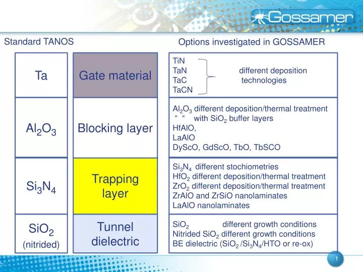
Standard TANOS. Options investigated in GOSSAMER. Ta. Gate material. TiN TaN different deposition TaC technologies TaCN. Al 2 O 3. Blocking layer. Al 2 O 3 different deposition/thermal treatment “ “ with SiO 2 buffer layers HfAlO ,

E N D
Standard TANOS Options investigated in GOSSAMER Ta Gate material TiN TaN different deposition TaC technologies TaCN Al2O3 Blocking layer Al2O3 different deposition/thermal treatment “ “ with SiO2 buffer layers HfAlO, LaAlO DyScO, GdScO, TbO, TbSCO Si3N4 Trapping layer Si3N4 different stochiometries HfO2 different deposition/thermal treatment ZrO2 different deposition/thermal treatment ZrAlO and ZrSiOnanolaminates LaAlOnanolaminates SiO2 (nitrided) Tunnel dielectric SiO2 different growth conditions Nitrided SiO2 different growth conditions BE dielectric (SiO2 /Si3N4/HTO or re-ox)
1Gb TANOS demonstrator RAM 500Mbit array 500Mbit array Numonyx inserted the Charge Trap cell into a 1Gbit 1.8V NAND device adapting cell pitch at row and column decoders thanks to an advanced copper metallization The device includes 1.8 billion cells but only 1 G is addressable due to the re-use of an existing cell design. Picture of 1Gbit NAND Charge Trap Flash Schematic layout ~40nm 2
22nm demonstration 4Mbit addressable array at 25nm • In Self-Aligned structure, W narrowing increases P/E efficiency • Down to 1x nm node we estimate no significant degradation of P/E windows
3-D architectures Multi-plane architecture Vertical SONOS Cell(imec) • - Effect of floating body channel • Effect of poly-silicon channel • Effect of wrap-around SONOS cell gate 25nm 30nm OXIDE Program v.s. diameter programming voltage